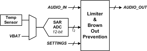
The TAS2770 monitors battery voltage (VBAT) and the audio signal to automatically decrease gain when the audio signal peaks exceed a programmable threshold. This helps prevent clipping and extends playback time through end of charge battery conditions. The limiter threshold can be configured to track VBAT below a programmable inflection point with a programmable slope. A minimum threshold sets the limit of threshold reduction from VBAT tracking. Configurable attack rate, hold time and release rate are provided to shape the dynamic response of the limiter (through the LIM_ATK_RT[2:0], LIM_HLD_TM[2:0] and LIM_RLS_RT[2:0] register bits).
A Brown Out Prevention (BOP) feature provides a priority input to the limiter to provide very fast response to transient dips in VBAT at end of charge conditions that can cause system level brown out. When VBAT dips below the BOP threshold, the limiter begins reducing gain with an attack latency of less than 10 µs and a configurable attack rate. When VBAT rises above the BOP threshold, the limiter will begin to release after the programmed hold time.
The limiter is enabled by setting the LIM_EN bit register bit high.
Table 8-44 Battery Tracking Limiter Enable| LIM_EN | Value |
|---|
0
| Disabled (default) |
1
| Enabled |
The limiter has configurable attack rate, hold time and release rate, which are available through the LIM_ATK_RT[2:0], LIM_HLD_TM[2:0] and LIM_RLS_RT[2:0] register bits respectively. The limiter attack and release step size can be set by configuring the LIM_ATK_ST[1:0] and LIM_RLS_ST[1:0] register bits respectively.
Table 8-45 Limiter Attack Rate| LIM_ATK_RT[2:0] | Attack Rate (µs) |
|---|
0x0
| 5 |
0x1
| 10 |
0x2
| 20 (default) |
0x3
| 40 |
0x4
| 80 |
0x5
| 160 |
0x6
| 320 |
0x7
| 640 |
Table 8-46 Limiter Hold Time| LIM_HLD_TM[2:0] | Hold Time (ms) |
|---|
0x0
| 0 |
0x1
| 10 |
0x2
| 25 |
0x3
| 50 |
0x4
| 100 |
0x5
| 250 |
0x6
| 500 (default) |
0x7
| 1000 |
Table 8-47 Limiter Release Rate| LIM_RLS_RT[2:0] | Release Time (ms) |
|---|
0x0
| 10 |
0x1
| 50 |
0x2
| 100 |
0x3
| 250 |
0x4
| 500 |
0x5
| 750 |
0x6
| 1000 (default) |
0x7
| 1500 |
Table 8-48 Limiter Attack Step Size| LIM_ATK_ST[1:0] | Step Size (dB) |
|---|
00
| 0.25 |
01
| 0.5 (default) |
10
| 1 |
11
| 2 |
Table 8-49 Limiter Release Step Size| LIM_RLS_ST[1:0] | Step Size (dB) |
|---|
00
| 0.25 |
01
| 0.5 (default) |
10
| 1 |
11
| 2 |
A maximum level of attenuation applied by the limiter and brown out prevention feature is configurable through the LIM_MAX_ATN[4:0] register bits. This attenuation limit is shared between the features. For instance, if the maximum attenuation is set to 6 dB and the limiter has reduced gain by 4 dB, the brown out prevention feature will only be able to reduce the gain further by another 2 dB. If the limiter or brown out prevention feature is attacking and it reaches the maximum attenuation, gain will not be reduced any further.
Table 8-50 Limiter Max Attenuation| LIM_MAX_ATN[4:0] | Attenuation (dB) |
|---|
0x00
| 1 |
0x01
| 1.5 |
...
| ... |
0x10
| 9 (default) |
...
| ... |
0x1E
| 16 |
0x1F
| 16.5 |
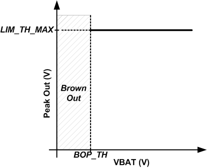
The limiter begins reducing gain when the output signal level is greater than the limiter threshold. The limiter can be configured to track VBAT below a programmable inflection point with a minimum threshold value. Figure 8-12 below shows the limiter configured to limit to a constant level regardless of VBAT level. To achieve this behavior, set the limiter maximum threshold to the desired level through the LIM_TH_MAX[6:0] register bits. Set the limiter inflection point (through the LIM_INF_PT[6:0] register bits) below the minimum allowable VBAT setting. The limiter minimum threshold register bits (LIM_TH_MIN[6:0]) do not impact limiter behavior in this use case.
Table 8-51 Limiter Maximum Threshold| LIM_TH_MAX[6:0] | Threshold (V) |
|---|
0x00
| 2 |
0x01
| 2.1 |
...
| ... |
0x6E
| 13 (default) |
...
| ... |
0x7E
| 14.6 |
0x7F
| 14.7 |
Table 8-52 Limiter Minimum Threshold| LIM_TH_MIN[6:0] | Threshold (V) |
|---|
0x00
| 2 |
0x01
| 2.1 |
...
| ... |
0x1E
| 5 (default) |
...
| ... |
0x7E
| 14.6 |
0x7F
| 14.7 |
Table 8-53 Limiter Inflection Point| LIM_INF_PT[6:0] | Inflection Point (V) |
|---|
0x00
| 2 |
0x01
| 2.1 |
...
| ... |
0x58
| 10.8 (default) |
...
| ... |
0x7E
| 14.6 |
0x7F
| 14.7 |
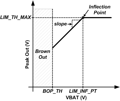
Figure 8-13 shows how to configure the limiter to track VBAT below a threshold without a minimum threshold. Set the LIM_TH_MAX[6:0] register bits to the desired threshold and LIM_INF_PT[6:0] register bits to the desired inflection point where the limiter will begin reducing the threshold with VBAT. The LIM_SLOPE[1:0] register bits can be used to change the slope of the limiter tracking with VBAT. The default value of 1 V/V will reduce the threshold 1 V for every 1 V of drop in VBAT. More aggressive tracking slopes can be programmed if desired. Program the LIM_TH_MIN[6:0] below the minimum VBAT to prevent the limiter from having a minimum threshold reduction when tracking VBAT.
Table 8-54 Limiter VBAT Tracking Slope| LIM_SLOPE[1:0] | Slope (V/V) |
|---|
00
| 1 (default) |
01
| 1.5 |
10
| 2 |
11
| 4 |
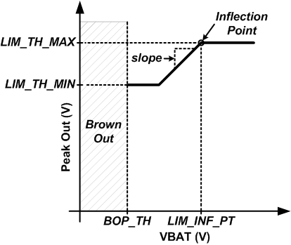
To achieve a limiter that tracks VBAT below a threshold, configure the limiter as explained in the previous example, except program the LIM_TH_MIN[6:0] register bits to the desired minimum threshold. This is shown in Figure 8-14 below.
The TAS2770 also employs a Brown Out Prevention (BOP) feature that serves as a low latency priority input to the limiter engine that begins attacking within 10 µs of VBAT dipping below the programmed BOP threshold. This feature can be enabled by setting the BOP_EN register bit high. It should be noted that the BOP feature is independent of the limiter and will function if enabled even if the limiter is disabled. The BOP threshold is configured by setting the threshold with register bits BOP_TH[7:0].
Table 8-55 Brown Out Prevention Enable| BOP_EN | Value |
|---|
0
| Disabled |
1
| Enabled (default) |
Table 8-56 Brown Out Prevention Threshold| BOP_TH[7:0] | Threshold (V) |
|---|
0x00
| 4.5 |
0x01
| 4.525 |
0x02
| 4.55 |
...
| ... |
0x14
| 5.0 (default) |
...
| ... |
0xFE
| 10.85 |
0xFF
| 10.875 |
The BOP feature has a separate attack rate, attack step size and hold time from the battery tracking limiter (register bits BOP_ATK_RT[2:0], BOP_ATK_ST[1:0] and BOP_HLD_TM[2:0] respectively). The BOP feature uses the LIM_RLS_RT[2:0] register setting to release after a brown out event.
Table 8-57 Brown Out Prevention Attack Rate| BOP_ATK_RT[2:0] | Attack Rate (µs) |
|---|
0x0
| 5 |
0x1
| 10 |
0x2
| 20 (default) |
0x3
| 40 |
0x4
| 80 |
0x5
| 160 |
0x6
| 320 |
0x7
| 640 |
Table 8-58 Brown Out Prevention Attack Step Size| BOP_ATK_ST[1:0] | Step Size (dB) |
|---|
00
| 0.5 |
01
| 1 (default) |
10
| 1.5 |
11
| 2 |
Table 8-59 Brown Out Prevention Hold Time| BOP_HLD_TM[2:0] | Hold Time (ms) |
|---|
0x0
| 0 |
0x1
| 10 |
0x2
| 25 |
0x3
| 50 |
0x4
| 100 |
0x5
| 250 |
0x6
| 500 (default) |
0x7
| 1000 |
The TAS2770 can also shutdown the device when a brown out event occurs if the BOP_SHUTDOWN register bit is set high. For the device to continue playing audio again, the device must transition through a SW/HW shutdown state. Setting the BOP_INF_HLD high will cause the limiter to stay in the hold state (i.e. never release) after a cleared brown out event until either the device transitions through a mute or SW/HW shutdown state or the register bit BOP_HLD_CLR is written to a high value (which will cause the device to exit the hold state and begin releasing). This bit is self clearing and will always readback low. Figure 8-16 below illustrates the entering and exiting from a brown out event.
Table 8-60 Shutdown on Brown Out Event| BOP_SHUTDOWN | Value |
|---|
0
| Don't Shutdown (default) |
1
| Shutdown |
Table 8-61 Infinite Hold on Brown Out Event| BOP_INF_HLD | Value |
|---|
0
| Use BOP_HLD_TM after Brown Out event (default) |
1
| Do not release until BOP_HLD_CLR is asserted high |
Table 8-62 BOP Infinite Hold Clear| BOP_HLD_CLR | Value |
|---|
0
| Don't clear (default) |
1
| Clear event (self clearing) |
 Figure 8-11 Limiter and Brown Out Prevention Interaction Diagram
 Figure 8-12 Limiter with Fixed Threshold
 Figure 8-13 Limiter with Inflection Point
 Figure 8-14 Limiter with Inflection Point and Minimum Threshold
 Figure 8-15 Limiter Block Diagram
 Figure 8-16 Brown Out Prevention Event