ZHCSIA0A May   2018  – November 2018 TAS3251

PRODUCTION DATA.  

  1. 特性
  2. 应用
  3. 说明
    1.     简化原理图
  4. 修订历史记录
  5. Device Comparison Table
  6. Pin Configuration and Functions
    1.     Pin Functions
  7. Specifications
    1. 7.1  Absolute Maximum Ratings
    2. 7.2  ESD Ratings
    3. 7.3  Recommended Operating Conditions
    4. 7.4  Thermal Information
    5. 7.5  Amplifier Electrical Characteristics
    6. 7.6  DAC Electrical Characteristics
    7. 7.7  Audio Characteristics (BTL)
    8. 7.8  Audio Characteristics (PBTL)
    9. 7.9  MCLK Timing
    10. 7.10 Serial Audio Port Timing – Slave Mode
    11. 7.11 Serial Audio Port Timing – Master Mode
    12. 7.12 I2C Bus Timing –Standard
    13. 7.13 I2C Bus Timing –Fast
    14. 7.14 Timing Diagrams
    15. 7.15 Typical Characteristics
      1. 7.15.1 BTL Configuration
      2. 7.15.2 PBTL Configuration
  8. Detailed Description
    1. 8.1 Overview
    2. 8.2 Functional Block Diagram
    3. 8.3 Feature Description
      1. 8.3.1  Power-on-Reset (POR) Function
      2. 8.3.2  Enable Device
      3. 8.3.3  DAC and DSP Clocking
        1. 8.3.3.1 Internal Clock Error Notification (CLKE)
      4. 8.3.4  Serial Audio Port
        1. 8.3.4.1 Clock Master Mode from Audio Rate Master Clock
        2. 8.3.4.2 Clock Slave Mode with 4-Wire Operation (SCLK, MCLK, LRCK/FS, SDIN)
        3. 8.3.4.3 Clock Slave Mode with SCLK PLL to Generate Internal Clocks (3-Wire PCM)
          1. 8.3.4.3.1 Clock Generation Using the PLL
          2. 8.3.4.3.2 PLL Calculation
            1. 8.3.4.3.2.1 Examples:
        4. 8.3.4.4 Serial Audio Port – Data Formats and Bit Depths
          1. 8.3.4.4.1 Data Formats and Master/Slave Modes of Operation
        5. 8.3.4.5 Input Signal Sensing (Power-Save Mode)
      5. 8.3.5  Volume Control
        1. 8.3.5.1 DAC Digital Gain Control
          1. 8.3.5.1.1 Emergency Volume Ramp Down
      6. 8.3.6  SDOUT Port and Hardware Control Pin
      7. 8.3.7  I2C Communication Port
        1. 8.3.7.1 Slave Address
        2. 8.3.7.2 Register Address Auto-Increment Mode
        3. 8.3.7.3 Packet Protocol
        4. 8.3.7.4 Write Register
        5. 8.3.7.5 Read Register
        6. 8.3.7.6 DSP Book, Page, and Register Update
          1. 8.3.7.6.1 Book and Page Change
          2. 8.3.7.6.2 Swap Flag
          3. 8.3.7.6.3 Example Use
      8. 8.3.8  Pop and Click Free Startup and Shutdown
      9. 8.3.9  Integrated Oscillator for Output Power Stage
        1. 8.3.9.1 Oscillator Synchronization and Slave Mode
      10. 8.3.10 Device Output Stage Protection System
        1. 8.3.10.1 Error Reporting
        2. 8.3.10.2 Overload and Short Circuit Current Protection
        3. 8.3.10.3 Signal Clipping and Pulse Injector
        4. 8.3.10.4 DC Speaker Protection
        5. 8.3.10.5 Pin-to-Pin Short Circuit Protection (PPSC)
        6. 8.3.10.6 Overtemperature Protection OTW and OTE
        7. 8.3.10.7 Undervoltage Protection (UVP) and Power-on Reset (POR)
        8. 8.3.10.8 Fault Handling
        9. 8.3.10.9 Output Power Stage Reset
      11. 8.3.11 Initialization, Startup and Shutdown
        1. 8.3.11.1 Power Up and Startup Sequence
        2. 8.3.11.2 Power Down and Shutdown Sequence
        3. 8.3.11.3 Device Mute
        4. 8.3.11.4 Device Unmute
        5. 8.3.11.5 Device Reset
        6. 8.3.11.6 Mute with DAC_MUTE or Clock Error
          1. 8.3.11.6.1 Mute using DAC_MUTE
        7. 8.3.11.7 Mute using Serial Audio Port Clock
        8. 8.3.11.8 Muting before an Unplanned Shutdown with DAC_MUTE
        9. 8.3.11.9 Output Power Stage Startup Timing
    4. 8.4 Device Functional Modes
      1. 8.4.1 Serial Audio Port Operating Modes
        1. 8.4.1.1 Master and Slave Mode Clocking for Digital Serial Audio Port
      2. 8.4.2 Communication Port Operating Modes
      3. 8.4.3 Speaker Amplifier Operating Modes
        1. 8.4.3.1 Stereo Mode
        2. 8.4.3.2 Mono Mode
    5. 8.5 Programming
      1. 8.5.1 Audio Processing Features
      2. 8.5.2 Processing Block Description
        1. 8.5.2.1  Input Scale and Mixer
          1. 8.5.2.1.1 Example
        2. 8.5.2.2  Sample Rate Converter
        3. 8.5.2.3  Parametric Equalizers (PEQ)
        4. 8.5.2.4  BQ Gain Scale
        5. 8.5.2.5  Dynamic Parametric Equalizer (DPEQ)
        6. 8.5.2.6  Two-Band Dynamic Range Control
        7. 8.5.2.7  Automatic Gain Limiter
          1. 8.5.2.7.1 Softening Filter Alpha (AEA)
          2. 8.5.2.7.2 Softening Filter Omega (AEO)
          3. 8.5.2.7.3 Attack Rate
          4. 8.5.2.7.4 Release Rate
          5. 8.5.2.7.5 Attack Threshold
        8. 8.5.2.8  Fine Volume
        9. 8.5.2.9  THD Boost
        10. 8.5.2.10 Level Meter
      3. 8.5.3 Other Processing Block Features
        1. 8.5.3.1 Number Format
          1. 8.5.3.1.1 Coefficient Format Conversion
      4. 8.5.4 Checksum
        1. 8.5.4.1 Cyclic Redundancy Check (CRC) Checksum
        2. 8.5.4.2 Exclusive or (XOR) Checksum
    6. 8.6 Register Maps
      1. 8.6.1 Registers - Page 0
        1. 8.6.1.1  Register 1 (0x01)
          1. Table 32. Register 1 (0x01) Field Descriptions
        2. 8.6.1.2  Register 2 (0x02)
          1. Table 33. Register 2 (0x02) Field Descriptions
        3. 8.6.1.3  Register 3 (0x03)
          1. Table 34. Register 3 (0x03) Field Descriptions
        4. 8.6.1.4  Register 4 (0x04)
          1. Table 35. Register 4 (0x04) Field Descriptions
        5. 8.6.1.5  Register 6 (0x06)
          1. Table 36. Register 6 (0x06) Field Descriptions
        6. 8.6.1.6  Register 7 (0x07)
          1. Table 37. Register 7 (0x07) Field Descriptions
        7. 8.6.1.7  Register 8 (0x08)
          1. Table 38. Register 8 (0x08) Field Descriptions
        8. 8.6.1.8  Register 9 (0x09)
          1. Table 39. Register 9 (0x09) Field Descriptions
        9. 8.6.1.9  Register 12 (0x0C)
          1. Table 40. Register 12 (0x0C) Field Descriptions
        10. 8.6.1.10 Register 13 (0x0D)
          1. Table 41. Register 13 (0x0D) Field Descriptions
        11. 8.6.1.11 Register 14 (0x0E)
          1. Table 42. Register 14 (0x0E) Field Descriptions
        12. 8.6.1.12 Register 15 (0x0F)
          1. Table 43. Register 15 (0x0F) Field Descriptions
        13. 8.6.1.13 Register 16 (0x10)
          1. Table 44. Register 16 (0x10) Field Descriptions
        14. 8.6.1.14 Register 17 (0x11)
          1. Table 45. Register 17 (0x11) Field Descriptions
        15. 8.6.1.15 Register 18 (0x12)
          1. Table 46. Register 18 (0x12) Field Descriptions
        16. 8.6.1.16 Register 20 (0x14)
          1. Table 47. Register 20 (0x14) Field Descriptions
        17. 8.6.1.17 Register 21 (0x15)
          1. Table 48. Register 21 (0x15) Field Descriptions
        18. 8.6.1.18 Register 22 (0x16)
          1. Table 49. Register 22 (0x16) Field Descriptions
        19. 8.6.1.19 Register 23 (0x17)
          1. Table 50. Register 23 (0x17) Field Descriptions
        20. 8.6.1.20 Register 24 (0x18)
          1. Table 51. Register 24 (0x18) Field Descriptions
        21. 8.6.1.21 Register 27 (0x1B)
          1. Table 52. Register 27 (0x1B) Field Descriptions
        22. 8.6.1.22 Register 28 (0x1C)
          1. Table 53. Register 28 (0x1C) Field Descriptions
        23. 8.6.1.23 Register 29 (0x1D)
          1. Table 54. Register 29 (0x1D) Field Descriptions
        24. 8.6.1.24 Register 30 (0x1E)
          1. Table 55. Register 30 (0x1E) Field Descriptions
        25. 8.6.1.25 Register 32 (0x20)
          1. Table 56. Register 32 (0x20) Field Descriptions
        26. 8.6.1.26 Register 33 (0x21)
          1. Table 57. Register 33 (0x21) Field Descriptions
        27. 8.6.1.27 Register 34 (0x22)
          1. Table 58. Register 34 (0x22) Field Descriptions
        28. 8.6.1.28 Register 37 (0x25)
          1. Table 59. Register 37 (0x25) Field Descriptions
        29. 8.6.1.29 Register 40 (0x28)
          1. Table 60. Register 40 (0x28) Field Descriptions
        30. 8.6.1.30 Register 41 (0x29)
          1. Table 61. Register 41 (0x29) Field Descriptions
        31. 8.6.1.31 Register 42 (0x2A)
          1. Table 62. Register 42 (0x2A) Field Descriptions
        32. 8.6.1.32 Register 43 (0x2B)
          1. Table 63. Register 43 (0x2B) Field Descriptions
        33. 8.6.1.33 Register 44 (0x2C)
          1. Table 64. Register 44 (0x2C) Field Descriptions
        34. 8.6.1.34 Register 59 (0x3B)
          1. Table 65. Register 59 (0x3B) Field Descriptions
        35. 8.6.1.35 Register 60 (0x3C)
          1. Table 66. Register 60 (0x3C) Field Descriptions
        36. 8.6.1.36 Register 61 (0x3D)
          1. Table 67. Register 61 (0x3D) Field Descriptions
        37. 8.6.1.37 Register 62 (0x3E)
          1. Table 68. Register 62 (0x3E) Field Descriptions
        38. 8.6.1.38 Register 63 (0x3F)
          1. Table 69. Register 63 (0x3F) Field Descriptions
        39. 8.6.1.39 Register 64 (0x40)
          1. Table 70. Register 64 (0x40) Field Descriptions
        40. 8.6.1.40 Register 65 (0x41)
          1. Table 71. Register 65 (0x41) Field Descriptions
        41. 8.6.1.41 Register 67 (0x43)
          1. Table 72. Register 67 (0x43) Field Descriptions
        42. 8.6.1.42 Register 68 (0x44)
          1. Table 73. Register 68 (0x44) Field Descriptions
        43. 8.6.1.43 Register 69 (0x45)
          1. Table 74. Register 69 (0x45) Field Descriptions
        44. 8.6.1.44 Register 70 (0x46)
          1. Table 75. Register 70 (0x46) Field Descriptions
        45. 8.6.1.45 Register 71 (0x47)
          1. Table 76. Register 71 (0x47) Field Descriptions
        46. 8.6.1.46 Register 72 (0x48)
          1. Table 77. Register 72 (0x48) Field Descriptions
        47. 8.6.1.47 Register 73 (0x49)
          1. Table 78. Register 73 (0x49) Field Descriptions
        48. 8.6.1.48 Register 74 (0x4A)
          1. Table 79. Register 74 (0x4A) Field Descriptions
        49. 8.6.1.49 Register 75 (0x4B)
          1. Table 80. Register 75 (0x4B) Field Descriptions
        50. 8.6.1.50 Register 76 (0x4C)
          1. Table 81. Register 76 (0x4C) Field Descriptions
        51. 8.6.1.51 Register 78 (0x4E)
          1. Table 82. Register 78 (0x4E) Field Descriptions
        52. 8.6.1.52 Register 79 (0x4F)
          1. Table 83. Register 79 (0x4F) Field Descriptions
        53. 8.6.1.53 Register 85 (0x55)
          1. Table 84. Register 85 (0x55) Register Field Descriptions
        54. 8.6.1.54 Register 86 (0x56)
          1. Table 85. Register 86 (0x56) Register Field Descriptions
        55. 8.6.1.55 Register 87 (0x57)
          1. Table 86. Register 87 (0x57) Field Descriptions
        56. 8.6.1.56 Register 88 (0x58)
          1. Table 87. Register 88 (0x58) Field Descriptions
        57. 8.6.1.57 Register 91 (0x5B)
          1. Table 88. Register 91 (0x5B) Field Descriptions
        58. 8.6.1.58 Register 92 (0x5C)
          1. Table 89. Register 92 (0x5C) Field Descriptions
        59. 8.6.1.59 Register 93 (0x5D)
          1. Table 90. Register 93 (0x5D) Field Descriptions
        60. 8.6.1.60 Register 94 (0x5E)
          1. Table 91. Register 94 (0x5E) Field Descriptions
        61. 8.6.1.61 Register 95 (0x5F)
          1. Table 92. Register 95 (0x5F) Field Descriptions
        62. 8.6.1.62 Register 108 (0x6C)
          1. Table 93. Register 108 (0x6C) Field Descriptions
        63. 8.6.1.63 Register 119 (0x77)
          1. Table 94. Register 119 (0x77) Field Descriptions
        64. 8.6.1.64 Register 120 (0x78)
          1. Table 95. Register 120 (0x78) Field Descriptions
      2. 8.6.2 Registers - Page 1
        1. 8.6.2.1 Register 1 (0x01)
          1. Table 96. Register 1 (0x01) Field Descriptions
        2. 8.6.2.2 Register 2 (0x02)
          1. Table 97. Register 2 (0x02) Field Descriptions
        3. 8.6.2.3 Register 6 (0x06)
          1. Table 98. Register 6 (0x06) Field Descriptions
        4. 8.6.2.4 Register 7 (0x07)
          1. Table 99. Register 7 (0x07) Field Descriptions
        5. 8.6.2.5 Register 9 (0x09)
          1. Table 100. Register 9 (0x09) Field Descriptions
  9. Application and Implementation
    1. 9.1 Typical Applications
      1. 9.1.1 Stereo, Bridge Tied Load (BTL) Application
      2. 9.1.2 Mono, Parallel Bridge-Tied Load (PBTL) Application
        1. 9.1.2.1 Parallel Bridge-Tied Load (PBTL), Pre-Filter
        2. 9.1.2.2 Parallel Bridge-Tied Load, Post-Filter
      3. 9.1.3 Design Requirements
      4. 9.1.4 Detailed Design Procedure
        1. 9.1.4.1 Step One: Schematic and Layout Design
          1. 9.1.4.1.1 Decoupling Capacitor Recommendations
          2. 9.1.4.1.2 PVDD Capacitor Recommendations
          3. 9.1.4.1.3 BST Capacitors
          4. 9.1.4.1.4 Heatsink
        2. 9.1.4.2 Step Two: Configure the Fixed-Function Process Flow for Use with the Target System
        3. 9.1.4.3 Step Three: Software Integration
      5. 9.1.5 Two TAS3251 Device Configurations
        1. 9.1.5.1 2 x PBTL Application
        2. 9.1.5.2 2 x BTL + 1 x PBTL Application
      6. 9.1.6 Three or More TAS3251 Device Configurations
      7. 9.1.7 Application Curves
  10. 10Power Supply Recommendations
    1. 10.1 Power Supplies
      1. 10.1.1 DAC_DVDD and DAC_AVDD Supplies
        1. 10.1.1.1 CPVSS, CN and CP Charge Pump
      2. 10.1.2 VDD Supply
      3. 10.1.3 GVDD_X Supply
      4. 10.1.4 PVDD Supply
      5. 10.1.5 BST Supply
  11. 11Layout
    1. 11.1 Layout Guidelines
      1. 11.1.1 General Guidelines for TAS3251
      2. 11.1.2 Importance of PVDD Bypass Capacitor Placement
    2. 11.2 Layout Examples
      1. 11.2.1 Bridge-Tied Load (BTL) Layout Example
      2. 11.2.2 Parallel Bridge-Tied Load (PBTL), Pre-Filter
      3. 11.2.3 Parallel Bridge-Tied Load (PBTL), Post-Filter
  12. 12器件和文档支持
    1. 12.1 器件支持
      1. 12.1.1 器件命名规则
      2. 12.1.2 开发支持
    2. 12.2 接收文档更新通知
    3. 12.3 社区资源
    4. 12.4 商标
    5. 12.5 静电放电警告
    6. 12.6 术语表
  13. 13机械、封装和可订购信息

封装选项

机械数据 (封装 | 引脚)
散热焊盘机械数据 (封装 | 引脚)
订购信息

SDOUT Port and Hardware Control Pin

The TAS3251 device contains a versatile GPIO port (SDOUT pin), allowing signals to be passed from the system to the device or sent from the device to the system. This pin can be used for advanced clocking features, to pass internal signals to the system or accept signals from the system for use inside the device by a given process flow.  The SDOUT pin supports serial data out and the features described in Figure 30. The register map can be used to configure the function of the SDOUT pin.

Here are a few key registers to enable the SDOUT pin:

  • Page 0, Register 7, Bit 0 (SDSL) - select if SDOUT data is pre-DSP or post-DSP processing.
  • Page 0, Register 9, Bit 5 (SDDIR) - select the SDOUT pin as input or output.
  • See register map for more details to configure the SDOUT pin function.
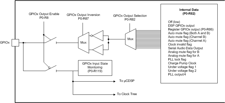
TAS3251 gpio_port_pins_slase71.gifFigure 30. SDOUT GPIO Port