ZHCSIA0A May 2018 – November 2018 TAS3251
PRODUCTION DATA.
- 1 特性
- 2 应用
- 3 说明
- 4 修订历史记录
- 5 Device Comparison Table
- 6 Pin Configuration and Functions
-
7 Specifications
- 7.1 Absolute Maximum Ratings
- 7.2 ESD Ratings
- 7.3 Recommended Operating Conditions
- 7.4 Thermal Information
- 7.5 Amplifier Electrical Characteristics
- 7.6 DAC Electrical Characteristics
- 7.7 Audio Characteristics (BTL)
- 7.8 Audio Characteristics (PBTL)
- 7.9 MCLK Timing
- 7.10 Serial Audio Port Timing – Slave Mode
- 7.11 Serial Audio Port Timing – Master Mode
- 7.12 I2C Bus Timing –Standard
- 7.13 I2C Bus Timing –Fast
- 7.14 Timing Diagrams
- 7.15 Typical Characteristics
-
8 Detailed Description
- 8.1 Overview
- 8.2 Functional Block Diagram
- 8.3
Feature Description
- 8.3.1 Power-on-Reset (POR) Function
- 8.3.2 Enable Device
- 8.3.3 DAC and DSP Clocking
- 8.3.4
Serial Audio Port
- 8.3.4.1 Clock Master Mode from Audio Rate Master Clock
- 8.3.4.2 Clock Slave Mode with 4-Wire Operation (SCLK, MCLK, LRCK/FS, SDIN)
- 8.3.4.3 Clock Slave Mode with SCLK PLL to Generate Internal Clocks (3-Wire PCM)
- 8.3.4.4 Serial Audio Port – Data Formats and Bit Depths
- 8.3.4.5 Input Signal Sensing (Power-Save Mode)
- 8.3.5 Volume Control
- 8.3.6 SDOUT Port and Hardware Control Pin
- 8.3.7 I2C Communication Port
- 8.3.8 Pop and Click Free Startup and Shutdown
- 8.3.9 Integrated Oscillator for Output Power Stage
- 8.3.10
Device Output Stage Protection System
- 8.3.10.1 Error Reporting
- 8.3.10.2 Overload and Short Circuit Current Protection
- 8.3.10.3 Signal Clipping and Pulse Injector
- 8.3.10.4 DC Speaker Protection
- 8.3.10.5 Pin-to-Pin Short Circuit Protection (PPSC)
- 8.3.10.6 Overtemperature Protection OTW and OTE
- 8.3.10.7 Undervoltage Protection (UVP) and Power-on Reset (POR)
- 8.3.10.8 Fault Handling
- 8.3.10.9 Output Power Stage Reset
- 8.3.11
Initialization, Startup and Shutdown
- 8.3.11.1 Power Up and Startup Sequence
- 8.3.11.2 Power Down and Shutdown Sequence
- 8.3.11.3 Device Mute
- 8.3.11.4 Device Unmute
- 8.3.11.5 Device Reset
- 8.3.11.6 Mute with DAC_MUTE or Clock Error
- 8.3.11.7 Mute using Serial Audio Port Clock
- 8.3.11.8 Muting before an Unplanned Shutdown with DAC_MUTE
- 8.3.11.9 Output Power Stage Startup Timing
- 8.4 Device Functional Modes
- 8.5
Programming
- 8.5.1 Audio Processing Features
- 8.5.2 Processing Block Description
- 8.5.3 Other Processing Block Features
- 8.5.4 Checksum
- 8.6
Register Maps
- 8.6.1
Registers - Page 0
- 8.6.1.1 Register 1 (0x01)
- 8.6.1.2 Register 2 (0x02)
- 8.6.1.3 Register 3 (0x03)
- 8.6.1.4 Register 4 (0x04)
- 8.6.1.5 Register 6 (0x06)
- 8.6.1.6 Register 7 (0x07)
- 8.6.1.7 Register 8 (0x08)
- 8.6.1.8 Register 9 (0x09)
- 8.6.1.9 Register 12 (0x0C)
- 8.6.1.10 Register 13 (0x0D)
- 8.6.1.11 Register 14 (0x0E)
- 8.6.1.12 Register 15 (0x0F)
- 8.6.1.13 Register 16 (0x10)
- 8.6.1.14 Register 17 (0x11)
- 8.6.1.15 Register 18 (0x12)
- 8.6.1.16 Register 20 (0x14)
- 8.6.1.17 Register 21 (0x15)
- 8.6.1.18 Register 22 (0x16)
- 8.6.1.19 Register 23 (0x17)
- 8.6.1.20 Register 24 (0x18)
- 8.6.1.21 Register 27 (0x1B)
- 8.6.1.22 Register 28 (0x1C)
- 8.6.1.23 Register 29 (0x1D)
- 8.6.1.24 Register 30 (0x1E)
- 8.6.1.25 Register 32 (0x20)
- 8.6.1.26 Register 33 (0x21)
- 8.6.1.27 Register 34 (0x22)
- 8.6.1.28 Register 37 (0x25)
- 8.6.1.29 Register 40 (0x28)
- 8.6.1.30 Register 41 (0x29)
- 8.6.1.31 Register 42 (0x2A)
- 8.6.1.32 Register 43 (0x2B)
- 8.6.1.33 Register 44 (0x2C)
- 8.6.1.34 Register 59 (0x3B)
- 8.6.1.35 Register 60 (0x3C)
- 8.6.1.36 Register 61 (0x3D)
- 8.6.1.37 Register 62 (0x3E)
- 8.6.1.38 Register 63 (0x3F)
- 8.6.1.39 Register 64 (0x40)
- 8.6.1.40 Register 65 (0x41)
- 8.6.1.41 Register 67 (0x43)
- 8.6.1.42 Register 68 (0x44)
- 8.6.1.43 Register 69 (0x45)
- 8.6.1.44 Register 70 (0x46)
- 8.6.1.45 Register 71 (0x47)
- 8.6.1.46 Register 72 (0x48)
- 8.6.1.47 Register 73 (0x49)
- 8.6.1.48 Register 74 (0x4A)
- 8.6.1.49 Register 75 (0x4B)
- 8.6.1.50 Register 76 (0x4C)
- 8.6.1.51 Register 78 (0x4E)
- 8.6.1.52 Register 79 (0x4F)
- 8.6.1.53 Register 85 (0x55)
- 8.6.1.54 Register 86 (0x56)
- 8.6.1.55 Register 87 (0x57)
- 8.6.1.56 Register 88 (0x58)
- 8.6.1.57 Register 91 (0x5B)
- 8.6.1.58 Register 92 (0x5C)
- 8.6.1.59 Register 93 (0x5D)
- 8.6.1.60 Register 94 (0x5E)
- 8.6.1.61 Register 95 (0x5F)
- 8.6.1.62 Register 108 (0x6C)
- 8.6.1.63 Register 119 (0x77)
- 8.6.1.64 Register 120 (0x78)
- 8.6.2 Registers - Page 1
- 8.6.1
Registers - Page 0
-
9 Application and Implementation
- 9.1
Typical Applications
- 9.1.1 Stereo, Bridge Tied Load (BTL) Application
- 9.1.2 Mono, Parallel Bridge-Tied Load (PBTL) Application
- 9.1.3 Design Requirements
- 9.1.4 Detailed Design Procedure
- 9.1.5 Two TAS3251 Device Configurations
- 9.1.6 Three or More TAS3251 Device Configurations
- 9.1.7 Application Curves
- 9.1
Typical Applications
- 10Power Supply Recommendations
- 11Layout
- 12器件和文档支持
- 13机械、封装和可订购信息
8.3.11.9 Output Power Stage Startup Timing
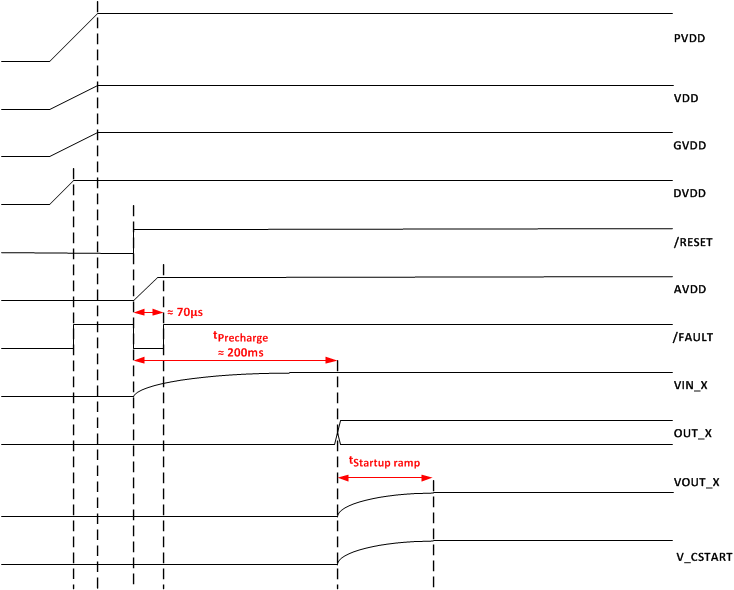
The TAS3251 output power stage does not require a specific power-up sequence, but it is recommended to hold RESET low for a minimum of 400 ms after PVDD supply voltage is powered on. The outputs of the half-bridges remain in a high-impedance state until the gate-drive supply voltage (GVDD_X) and VDD voltage are above the undervoltage protection (UVP) voltage threshold (see the Electrical Characteristics table of this data sheet). This allows an internal circuit to charge the external bootstrap capacitors by enabling a weak pull-down of the half-bridge output as well as initiating a controlled ramp up sequence of the output voltage.
 Figure 38. Power Stage Startup Timing
 When RESET is released to turn on TAS3251, FAULT signal will output low and AVDD voltage regulator will be enabled. FAULT will stay low until AVDD reaches the undervoltage protection (UVP) voltage threshold (see the Electrical Characteristics table of this data sheet). Next a pre-charge time begins to stabilize the DC voltage across the input AC coupling capacitors, followed by the ramp up output power stage sequence .