ZHCSFW8 December 2016 TAS5414C
PRODUCTION DATA.
- 1 特性
- 2 应用
- 3 说明
- 4 修订历史记录
- 5 Pin Configuration and Functions
- 6 Specifications
-
7 Detailed Description
- 7.1 Overview
- 7.2 Functional Block Diagram
- 7.3 Feature Descption
- 7.4 Device Functional Modes
- 7.5 Programming
- 7.6
Register Maps
- 7.6.1 Register Summary
- 7.6.2 Registers
- 7.6.3 Fault Register 2 (0x01) Protection
- 7.6.4 Diagnostic Register 1 (0x02) Load Diagnostics
- 7.6.5 Diagnostic Register 2 (0x03) Load Diagnostics
- 7.6.6 External Status Register 1 (0x04) Fault Detection
- 7.6.7 External Status Register 2 (0x05) Output State of Individual Channels
- 7.6.8 External Status Register 3 (0x06) Play and Mute Modes
- 7.6.9 External Status Register 4 (0x07) Load Diagnostics
- 7.6.10 External Control Register 1 (0x08) Gain Select
- 7.6.11 External Control Register 2 (0x09) Overcurrent Control
- 7.6.12 External Control Register 3 (0x0A) Switching Frequency Select and Clip_OTW Configuration
- 7.6.13 External Control Register 4 (0x0B) Load Diagnostics and Master/Slave Control
- 7.6.14 External Control Register 5 (0x0C) Output Control
- 7.6.15 External Control Register 6 (0x0D) Output Control
- 7.6.16 External Control Register 7 (0x10) Miscellaneous Selection
- 7.6.17 External Status Register 5 (0x13) Overtemperature and Thermal Foldback Status
- 8 Application and Implementation
- 9 Power Supply Recommendations
- 10Layout
- 11器件和文档支持
- 12机械、封装和可订购信息
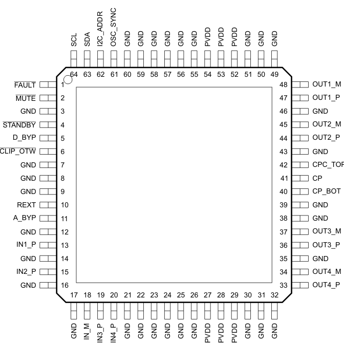
5 Pin Configuration and Functions
The pin assignments are shown as follows.
PHD Package
64-Pin HTQFP
Top View

Pin Functions
| PIN | TYPE(1) | DESCRIPTION | |
|---|---|---|---|
| NAME | TAS5414C PHD Package NO. |
||
| A_BYP | 11 | PBY | Bypass pin for the AVDD analog regulator |
| CLIP_OTW | 6 | DO | Reports CLIP, OTW, or both. It also reports tweeter detection during tweeter mode. Open-drain |
| CP | 41 | CP | Top of main storage capacitor for charge pump (bottom goes to PVDD) |
| CPC_BOT | 40 | CP | Bottom of flying capacitor for charge pump |
| CPC_TOP | 42 | CP | Top of flying capacitor for charge pump |
| D_BYP | 5 | PBY | Bypass pin for DVDD regulator output |
| FAULT | 1 | DO | Global fault output (open drain): UV, OV, OTSD, OCSD, DC |
| GND | 3, 7, 8, 9, 12, 14, 16, 17, 21, 22, 23, 24, 25, 26, 30, 31, 32, 35, 38, 39, 43, 46, 49, 50, 51, 55, 56, 57, 58, 59, 60 | GND | Ground |
| I2C_ADDR | 62 | AI | I2C address bit |
| IN1_P | 13 | AI | Non-inverting analog input for channel 1 |
| IN2_P | 15 | AI | Non-inverting analog input for channel 2 |
| IN3_P | 19 | AI | Non-inverting analog input for channel 3 |
| IN4_P | 20 | AI | Non-inverting analog input for channel 4 |
| IN_M | 18 | ARTN | Signal return for the four analog channel inputs (TAS5414C only) |
| MUTE | 2 | AI | Gain ramp control: mute (low), play (high) |
| OSC_SYNC | 61 | DI/DO | Oscillator input from master or output to slave amplifiers |
| OUT1_M | 48 | PO | – polarity output for bridge 1 |
| OUT1_P | 47 | PO | + polarity output for bridge 1 |
| OUT2_M | 45 | PO | – polarity output for bridge 2 |
| OUT2_P | 44 | PO | + polarity output for bridge 2 |
| OUT3_M | 37 | PO | – polarity output for bridge 3 |
| OUT3_P | 36 | PO | + polarity output for bridge 3 |
| OUT4_M | 34 | PO | – polarity output for bridge 4 |
| OUT4_P | 33 | PO | + polarity output for bridge 4 |
| PVDD | 27, 28, 29, 52, 53, 54 | PWR | PVDD supply |
| REXT | 10 | AI | Precision resistor pin to set analog reference |
| SCL | 64 | DI | I2C clock input from system I2C master |
| SDA | 63 | DI/DO | I2C data I/O for communication with system I2C master |
| STANDBY | 4 | DI | Active-low STANDBY pin. Standby (low), power up (high) |
(1) DI = digital input, DO = digital output, AI = analog input, ARTN = analog signal return, PWR = power supply, PBY = power bypass, PO = power output, GND = ground, CP = charge pump.