ZHCSFW8 December 2016 TAS5414C
PRODUCTION DATA.
- 1 特性
- 2 应用
- 3 说明
- 4 修订历史记录
- 5 Pin Configuration and Functions
- 6 Specifications
-
7 Detailed Description
- 7.1 Overview
- 7.2 Functional Block Diagram
- 7.3 Feature Descption
- 7.4 Device Functional Modes
- 7.5 Programming
- 7.6
Register Maps
- 7.6.1 Register Summary
- 7.6.2 Registers
- 7.6.3 Fault Register 2 (0x01) Protection
- 7.6.4 Diagnostic Register 1 (0x02) Load Diagnostics
- 7.6.5 Diagnostic Register 2 (0x03) Load Diagnostics
- 7.6.6 External Status Register 1 (0x04) Fault Detection
- 7.6.7 External Status Register 2 (0x05) Output State of Individual Channels
- 7.6.8 External Status Register 3 (0x06) Play and Mute Modes
- 7.6.9 External Status Register 4 (0x07) Load Diagnostics
- 7.6.10 External Control Register 1 (0x08) Gain Select
- 7.6.11 External Control Register 2 (0x09) Overcurrent Control
- 7.6.12 External Control Register 3 (0x0A) Switching Frequency Select and Clip_OTW Configuration
- 7.6.13 External Control Register 4 (0x0B) Load Diagnostics and Master/Slave Control
- 7.6.14 External Control Register 5 (0x0C) Output Control
- 7.6.15 External Control Register 6 (0x0D) Output Control
- 7.6.16 External Control Register 7 (0x10) Miscellaneous Selection
- 7.6.17 External Status Register 5 (0x13) Overtemperature and Thermal Foldback Status
- 8 Application and Implementation
- 9 Power Supply Recommendations
- 10Layout
- 11器件和文档支持
- 12机械、封装和可订购信息
8 Application and Implementation
NOTE
Information in the following applications sections is not part of the TI component specification, and TI does not warrant its accuracy or completeness. TI’s customers are responsible for determining suitability of components for their purposes. Customers should validate and test their design implementation to confirm system functionality.
8.1 Application Information
The TAS5414C is a four-channel Class-D audio amplifier designed for use in head units and external amplifier modules. The device incorporates all the functionality needed to perform in the demanding OEM applications area.
8.2 Typical Application
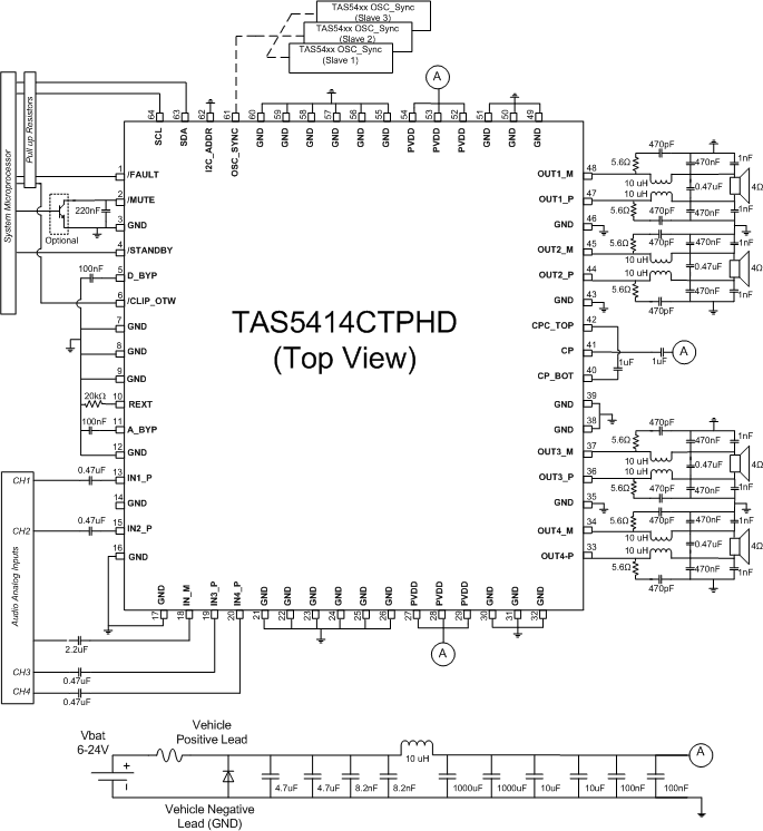
Figure 36 shows a typical application circuit for the TAS5414C.
 Figure 36. TAS5414C Typical Application Schematic
8.2.1 Design Requirements
- Power Supplies
- Communication
- External Components
The device needs only a single power supply compliant with the recommended operation range. The device is designed to work with either a vehicle battery or regulated boost power supply.
The device communicates with the system controller with both discrete hardware control pins and with I 2 C. The device is an I 2 C slave and thus requires a master. If a master I 2 C-compliant device is not present in the system, it is still possible to use the device, but only with the default settings. Diagnostic information is limited to the discrete reporting FAULT pin.
Table 24 lists the components required for the device.
Table 24. Supporting Components
| EVM Designator | Quanity | Value | Size | Description | Use in Application |
|---|---|---|---|---|---|
| C37, C39, C48, C52 | 4 | 0.47μF ± 10% | 1206 | Film, 16-V | Analog audio input filter, bypass |
| C5, C6, C7, C8 | 4 | 330 μF ± 20% | 10 mm | Low-ESR aluminum capacitor, 35-V | Power supply |
| C9, C10, C50, C51, C27, C28 | 6 | 1 μF ± 10% | 0805 | X7R ceramic capacitor, 50-V | Power supply |
| C53, C55 | 2 | 1uF ± 10% | 0805 | Film, 16-V | Analog audio input filter, bypass |
| C14, C23, C32, C43 | 4 | 470nF ± 10% | 0805 | X7R ceramic capacitor, 50-V | Amplifier output filtering |
| C11, C15, C20, C24, C29, C34, C40, C45 | 8 | 470 pF ± 10% | 0603 | X7R ceramic capacitor, 50-V | Amplifier output snubbers |
| C19, C33 | 2 | 0.1 μF ± 10% | 0603 | X7R ceramic capacitor, 25-V | Power supply |
| C4 | 1 | 2200 pF ± 10% | 0603 | X7R ceramic capacitor, 50-V | Power supply |
| C3 | 1 | 0.082 μF ± 10% | 0603 | X7R ceramic capacitor, 25-V | Power supply |
| C1, C2 | 2 | 4.7 μF ± 10% | 1206 | X7R ceramic capacitor, 25-V | Power supply |
| C12, C16, C21, C25, C30, C35, C41, C46 | 8 | 0.47 μF ± 10% | 0603 | X7R ceramic capacitor, 25-V | Output EMI filtering |
| C18 | 1 | 220nF ± 10% | 0603 | X7R ceramic capacitor, 25-V | Mute timing |
| L1 | 1 | 10 μH ± 20% | 13.5 mm ×13.5 mm | Shielded ferrite inductor | Power supply |
| L2, L3, L4, L5 | 4 | 10 μH ± 20% | 12 mm × 14 mm | Dual inductor | Amplifier output filtering |
| R5, R6, R7 | 3 | 49.9 kΩ ± 1% | 0805 | Resistors, 0.125-W | Analog audio input filter |
| R8, R10, R12, R14, R17, R19, R26, R29 | 8 | 5.6 Ω ± 5% | 0805 | Resistors, 0.125-W | Output snubbers |
| R16 | 1 | 20.0 kΩ ± 1% | 0805 | Resistors, 0.125-W | Power supply |
8.2.2 Detailed Design Procedure
8.2.2.1 Hardware and Software Design
- Step 1: Hardware Schematic Design: Using the Typical Application Schematic as a guide, integrate the hardware into the system schematic.
- Step 2: Following the recommended layout guidelines, integrate the device and its supporting components into the system PCB file.
- Step 3: Thermal Design: The device has an exposed thermal pad which requires proper soldering. For more information, see the Semiconductor and IC Package Thermal Metrics , SPRA953, and the PowerPAD Thermally Enhanced Package, SLMA002G, application reports.
- Step 4: Develop software: The EVM User's Guide has detailed instructions for how to set up the device, interpret diagnostic information, and so forth. For information about control registers, see the Table 7 section.
- For questions and support go to the E2E forums.
8.2.2.2 Parallel Operation (PBTL)
The device can drive more current by paralleling BTL channels on the load side of the LC output filter. Parallel operation requires identical I2C settings for any two paralleled channels in order to have reliable system performance and even power dissipation on multiple channels. For smooth power up, power down, and mute operation, the same control commands (such as mute, play, Hi-Z, and so on) should be sent to the paralleled channels at the same time. The device also supports load diagnostics for parallel connection. There is no support for paralleling on the device side of the LC output filter, which can result in device failure. When paralleling channels, use the parallel BTL I2C control bits in register 0x0D. Parallel channels 1 and 2, and/or channels 3 and 4. Setting these bits allows the thermal foldback to react on both channels equally. Provide the audio input to channel 2 if paralleing channels 1 and 2, and channel 3 if paralleling channels 3 and 4.
8.2.2.3 Input Filter Design
For the TAS5414C device, the IN_M pin should have an impedance to GND that is equivalent to the parallel combination of the input impedances of all IN_P channels combined, including any source impedance from the previous stage in the system design. For example, if each of the four IN_P channels have a 1-µF dc blocking capacitor, 1 kΩ of series resistance due to an input RC filter, and 1 kΩ of source resistance from the DAC supplying the audio signal, then the IN_M channel should have a 4-µF capacitor in series with a 500-Ω resistor to GND (4 × 1 µF in parallel = 4 µF; 4 × 2 kΩ in parallel = 500 Ω).
8.2.2.4 Amplifier Output Filtering
The output FETs drive the amplifier outputs in an H-bridge configuration. These transistors are either fully off or on. The result is a square-wave output signal with a duty cycle that is proportional to the amplitude of the audio signal. The amplifier outputs require a low-pass filter to filter out the PWM modulation carrier frequency. People frequently call this filter the L-C filter, due to the presence of an inductive element L and a capacitive element C to make up the 2-pole low-pass filter. The L-C filter attenuates the carrier frequency, reducing electromagnetic emissions and smoothing the current waveform which the load draws from the power supply. See the Class-D LC Filter Design application report, SLOA119 , for a detailed description on proper component selection and design of an L-C filter based upon the desired load and response.
8.2.2.5 Line Driver Applications
In many audio applications, the end user would like to use the same head unit to drive either a speaker (with several ohms of impedance) or an external amplifier (with several kilohms of impedance). The design is capable of supporting both applications; however, the one must design the output filter and system to handle the expected output load conditions.
8.2.3 Application Curves
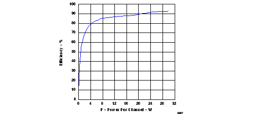
 Figure 37. Efficiency
Four Channels AT 4 Ω Each
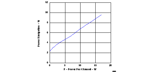
 Figure 38. Device Power Dissipation
Four Channels at 4 Ω Each