ZHCSB67B April 2013 – April 2015 TAS5558
PRODUCTION DATA.
- 1 特性
- 2 应用
- 3 说明
- 4 修订历史记录
- 5 Pin Configuration and Functions
-
6 Specifications
- 6.1 Absolute Maximum Ratings
- 6.2 ESD Ratings
- 6.3 Recommended Operating Conditions
- 6.4 Thermal Information
- 6.5 Electrical Characteristics
- 6.6 Dynamic Performance
- 6.7 SRC Performance
- 6.8 Timing I2C Serial Control Port Operation
- 6.9 Reset Timing (RESET)
- 6.10 Power-Down (PDN) Timing
- 6.11 Back-End Error (BKND_ERR)
- 6.12 Mute Timing (MUTE)
- 6.13 Headphone Select (HP_SEL)
- 6.14 Switching Characteristics - Clock Signals
- 6.15 Switching Characteristics - Serial Audio Port
- 6.16 Volume Control
- 6.17 Typical Characteristics
-
7 Detailed Description
- 7.1 Overview
- 7.2 Functional Block Diagram
- 7.3 Feature Description
- 7.4
Device Functional Modes
- 7.4.1 Power Supply
- 7.4.2 Clock, PLL, and Serial Data Interface
- 7.4.3 Serial Audio Interface
- 7.4.4 I 2C Serial-Control Interface
- 7.4.5 Device Control
- 7.4.6 Energy Manager
- 7.4.7 Digital Audio Processor (DAP)
- 7.4.8 Pulse Width Modulation Schemes
- 7.4.9 TAS5558 DAP Architecture Diagrams
- 7.4.10 I 2C Coefficient Number Formats
- 7.4.11 Input Crossbar Mixer
- 7.4.12 Biquad Filters
- 7.4.13 Bass and Treble Controls
- 7.4.14 Volume, Automute, and Mute
- 7.4.15 Loudness Compensation
- 7.4.16 Dynamic Range Control (DRC)
- 7.4.17 THD Manager
- 7.4.18 Downmix Algorithm and I2S Out
- 7.4.19 Stereo Downmixes/(or Fold-Downs)
- 7.4.20 Output Mixer
- 7.4.21 Device Configuration Controls
- 7.4.22 Master Clock and Serial Data Rate Controls
- 7.4.23 Bank Controls (ASRC Bypass only)
- 7.5 Programming
- 7.6
Register Maps
- 7.6.1 Serial-Control I2C Register Summary
- 7.6.2
Serial-Control Interface Register Definitions
- 7.6.2.1 Clock Control Register (0x00)
- 7.6.2.2 General Status Register 0 (0x01)
- 7.6.2.3 Error Status Register (0x02)
- 7.6.2.4 System Control Register 1 (0x03)
- 7.6.2.5 System Control Register 2 (0x04)
- 7.6.2.6 Channel Configuration Control Registers (0x05-0x0C)
- 7.6.2.7 Headphone Configuration Control Register (0x0D)
- 7.6.2.8 Serial Data Interface Control Register (0x0E)
- 7.6.2.9 Soft Mute Register (0x0F)
- 7.6.2.10 Energy Manager Status Register (0x10)
- 7.6.2.11 Automute Control Register (0x14)
- 7.6.2.12 Output Automute PWM Threshold and Back-End Reset Period Register (0x15)
- 7.6.2.13 Modulation Index Limit Register (0x16, 0x17, 0x18, 0x19)
- 7.6.2.14 AD Mode - 8 Interchannel Channel Delay and Global Offset Registers (0x1B to 0x23)
- 7.6.2.15 Special Low Z and Mid Z Ramp/Stop Period (0x24)
- 7.6.2.16 PWM and EMO Control Register (0x25)
- 7.6.2.17 Individual Channel Shutdown (0x27)
- 7.6.2.18 Input Mux Registers (0x30, 0x31, 0x32, 0x33)
- 7.6.2.19 PWM Mux Registers (0x34, 0x35, 0x36, 0x37)
- 7.6.2.20 BD Mode and Ternary - 8 Interchannel Channel Delay (0x38 to 0x3F)
- 7.6.2.21 Bank-Switching Command Register (0x40) (TAS5558 + ASRC Bypass)
- 7.6.2.22 Input Mixer Registers, Channels 1-8 (0x41-0x48)
- 7.6.2.23 Bass Mixer Registers (0x49-0x50)
- 7.6.2.24 Biquad Filter Register (0x51-0x88)
- 7.6.2.25 Bass and Treble Register, Channels 1-8 (0x89-0x90)
- 7.6.2.26 Loudness Registers (0x91-0x95)
- 7.6.2.27 DRC1 Control Register CH1-7 (0x96) - Write
- 7.6.2.28 DRC2 Control Register CH8 (0x97) - Write Register
- 7.6.2.29 DRC1 Data Registers (0x98-0x9C)
- 7.6.2.30 DRC2 Data Registers (0x9D-0xA1)
- 7.6.2.31 DRC Bypass Registers (0xA2-0xA9)
- 7.6.2.32 Output Select and Mix Registers 8x2 (0x-0xAF)
- 7.6.2.33 8×3 Output Mixer Registers (0xB0-0xB1)
- 7.6.2.34 ASRC Registers (0xC3-C5)
- 7.6.2.35 Auto Mute Behavior (0xCC)
- 7.6.2.36 PSVC Volume Biquad Register (0xCF)
- 7.6.2.37 Volume, Treble, and Bass Slew Rates Register (0xD0)
- 7.6.2.38 Volume Registers (0xD1-0xD9)
- 7.6.2.39 Bass Filter Set Register (0xDA)
- 7.6.2.40 Bass Filter Index Register (0xDB)
- 7.6.2.41 Treble Filter Set Register (0xDC)
- 7.6.2.42 Treble Filter Index (0xDD)
- 7.6.2.43 AM Mode Register (0xDE)
- 7.6.2.44 PSVC Range Register (0xDF)
- 7.6.2.45 General Control Register (0xE0)
- 7.6.2.46 96kHz Dolby Downmix Coefficients (0xE3 to 0xE8)
- 7.6.2.47 THD Manager Configuration (0xE9 and 0xEA)
- 7.6.2.48 SDIN5 Input Mixer (0xEC-0xF3)
- 7.6.2.49 192kHZ Process Flow Output Mixer (0xF4-0xF7)
- 7.6.2.50 192kHz Dolby Downmix Coefficients (0xFB and 0xFC)
- 8 Application and Implementation
- 9 Power Supply Recommendations
- 10Layout
- 11器件和文档支持
- 12机械封装和可订购信息
10 Layout
10.1 Layout Guidelines
- The TAS5558 uses the PCB as a heat sink; therefore, the PowerPAD must be soldered to the PCB, and adequate copper areas and copper vias connecting the top, bottom, and internal layers should be used.
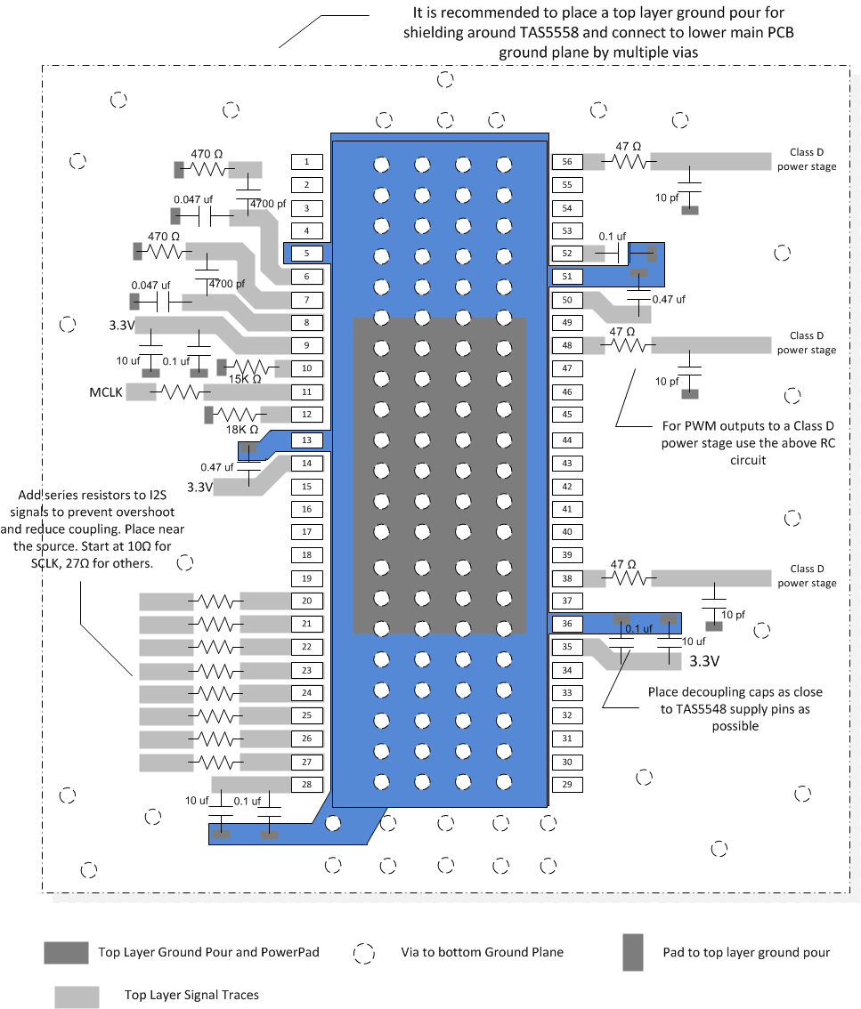
- Decoupling capacitors should be placed as close to the DVDD1_CORE, DVDD2_CORE, VR_DIG, AVDD_PWM and AVDD as possible. These decoupling capacitors should also have a path through the GND plane back to the power pad, as shown by the blue area in the layout example in Figure 53.
- A single common GND plane between AGND and DGND is recommended to avoid a potential voltage difference between them. Multiple vias from the TAS5558 PowerPAD should be connected to GND with a large copper pad as well as vias to all GND planes.
- Further guidelines can be found on the layout example in Figure 53.
- A more detailed example of the PCB layout can be found in the TAS5548EVM User's Guide (SLOU351).
10.2 Layout Example
 Figure 53. TAS5558 Layout Example
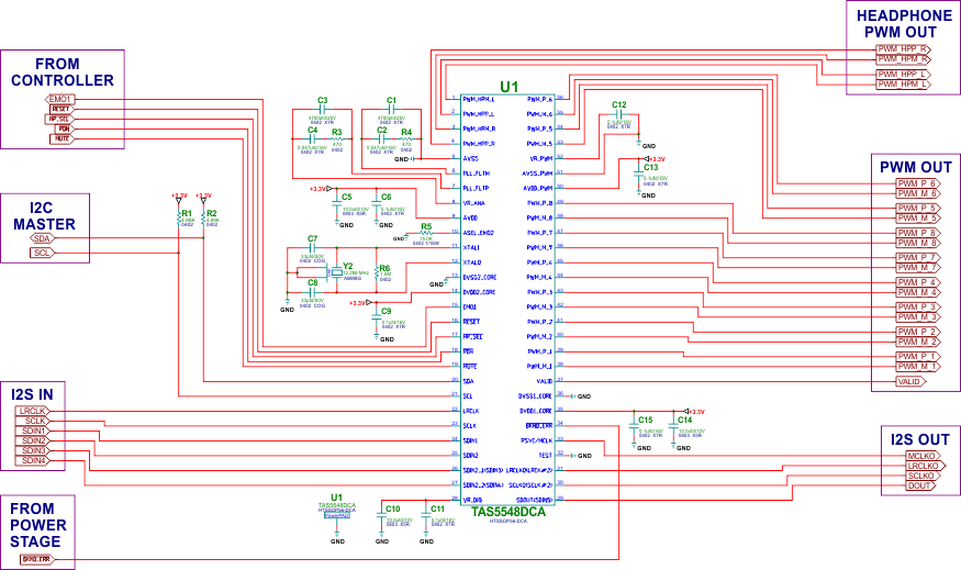
 Figure 54. Recommended External Components