ZHCS928A May 2012 – January 2016 TAS5624A
PRODUCTION DATA.
- 1 特性
- 2 应用
- 3 说明
- 4 修订历史记录
- 5 Device Comparison Table
- 6 Pin Configuration and Functions
-
7 Specifications
- 7.1 Absolute Maximum Ratings
- 7.2 ESD Ratings
- 7.3 Recommended Operating Conditions
- 7.4 Thermal Information
- 7.5 Electrical Characteristics
- 7.6 Electrical Characteristics - Audio Specification Stereo (BTL)
- 7.7 Electrical Characteristics - Audio Specification 4 Channels (SE)
- 7.8 Electrical Characteristics - Audio Specification Mono (PBTL)
- 7.9 Typical Characteristics
- 8 Parameter Measurement Information
-
9 Detailed Description
- 9.1 Overview
- 9.2 Functional Block Diagrams
- 9.3
Feature Description
- 9.3.1 System Power-Up and Power-Down Sequence
- 9.3.2 Start-Up and Shutdown Ramp Sequence
- 9.3.3 Unused Output Channels
- 9.3.4 Device Protection System
- 9.3.5 Pin-to-Pin Short-Circuit Protection (PPSC)
- 9.3.6 Overtemperature Protection
- 9.3.7 Overtemperature Warning, OTW
- 9.3.8 Undervoltage Protection (UVP) and Power-On Reset (POR)
- 9.3.9 Error Reporting
- 9.3.10 Fault Handling
- 9.3.11 Device Reset
- 9.3.12 System Design Consideration
- 9.4 Device Functional Modes
- 10Application and Implementation
- 11Power Supply Recommendations
- 12Layout
- 13器件和文档支持
- 14机械、封装和可订购信息
10 Application and Implementation
NOTE
Information in the following applications sections is not part of the TI component specification, and TI does not warrant its accuracy or completeness. TI’s customers are responsible for determining suitability of components for their purposes. Customers should validate and test their design implementation to confirm system functionality.
10.1 Application Information
These typical connection diagrams highlight the required external components and system level connections for proper operation of the device in several popular use cases. Each of these configurations can be realized using the evaluation modules (EVMs) for the device. These flexible modules allow full evaluation of the device in the most common modes of operation. Any design variation can be supported by TI through schematic and layout reviews. Visit the E2E Forum at www.e2e.ti.com for design assistance and join the audio amplifier discussion forum for additional information.
10.2 Typical Applications
10.2.1 Typical BTL Application
See Figure 16 for application schematic. In this application, differential PWM inputs are used with AD modulation from the PWM modulator (TAS5558). AD modulation scheme is defined as PWM(+) as opposite polarity from PWM(–).
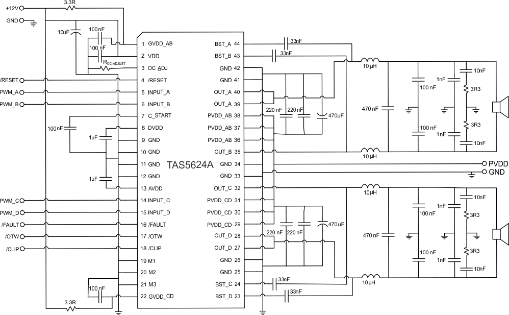 Figure 16. Typical Differential (2N) BTL Application With AD Modulation Filters
10.2.1.1 Design Requirements
Table 5 lists the design parameters of Figure 16.
Table 5. Design Requirements
| PARAMETER | VALUE |
|---|---|
| Digital regulator supply | 12 V |
| Full-bridge power supply | 12 V to 38 V |
| PWM modulator | TAS5558 |
| Output filters | Inductor-capacitor lowpass filter |
| Speaker | 2.5 Ω minimum |
10.2.1.2 Detailed Design Procedure
Using Figure 16 as a guide, integrate the hardware into the system schematic.
Following the recommended component placement, schematic layout and routing given in Layout Example, integrate the device and its supporting components into the system PCB file.
- The most critical section of the circuit is the power supply inputs, the amplifier output signals, and the high-frequency signals which go to the serial audio port. TI recommends that these be constructed to ensure they are given precedent as design trade-offs are made.
- For questions and support go to the E2E Forum at www.e2e.ti.com. If it is necessary to deviate from the recommended layout, please visit the E2E Forum to request a layout review.
10.2.1.2.1 Pin Connections
- Pin 1 - GVDD_AB is the gate-drive voltage for half-bridges A and B. It needs a 3.3-Ω isolation resistor and a 0.1-µF decoupling capacitor.
- Pin 2 - VDD is the supply for internal voltage regulators AVDD and DVDD. It needs a 10-µF bulk capacitor and a 0.1-µF decoupling capacitor.
- Pin 3 - Roc adjust is the overcurrent programming resistor. Depending on the application, this resistor can be between 24 kΩ to 68 kΩ.
- Pin 4 - RESET pin when asserted, it keeps outputs Hi-Z and no PWM switching. This pin can be controlled by a microprocessor.
- Pins 5 and 6 - These are PWM(+) and PWM(–) pins with signals provided by a PWM modulator such as the TAS5558. These are PWM differential pairs.
- Pin 7 - Start-up ramp capacitor must be 1 µF for SE configuration.
- Pin 8 - Digital output supply pin is connected to 1-µF decoupling capacitor.
- Pins 9-12 - Ground pins are connected to board ground.
- Pin 13 - Analog output supply pin is connected to 1-µF decoupling capacitor.
- Pins 14 and 15 - These are PWM(+) and PWM(–) pins with signals provided by a PWM modulator such as the TAS5558. These are PWM differential pair.
- Pin 16 - Fault pin can be monitored by a microcontroller through GPIO pin. System can decide to assert reset or shutdown.
- Pin 17 - Overtemperature warning pin can be monitored by a microcontroller through a GPIO pin. System can decide to turn on fan or lower output power.
- Pin 18 - Output clip indicator can be monitored by a microcontroller through a GPIO pin. System can decide to lower the volume.
- Pins 19-21 - Mode pins set the input and output configurations. For this configuration M1-M3 are grounded. These mode pins must be hardware configured, such as, not through GPIO pins from a microcontroller.
- Pin 22 - GVDD_CD is the gate-drive voltage for half-bridges C and D. This pin needs a 3.3-Ω isolation resistor and a 0.1-µF decoupling capacitor.
- Pins 23, 24, 43, 44 - Bootstrap pins for half-bridges A, B, C, and D. Connect 33 nF from this pin to corresponding output pins.
- Pins 25, 26, 33, 34, 41, 42 - These ground pins must be used to ground decoupling capacitors from PVDD_X.
- Pins 27, 28, 32, 35, 39, 40 - Output pins from half-bridges A, B, C, and D. Connect appropriate bootstrap capacitors and differential LC filter as shown in Figure 20.
- Pins 29, 30, 31, 36, 37, 38 - Power supply pins to half-bridges A, B, C, and D. A and B form a full-bridge and C and D form another full-bridge. A 470-µF bulk capacitor is recommended for each full-bridge power pins. Two 0.22-µF decoupling capacitors are placed on each full-bridge power pins. See Figure 20 for details.
10.2.1.3 Application Curves
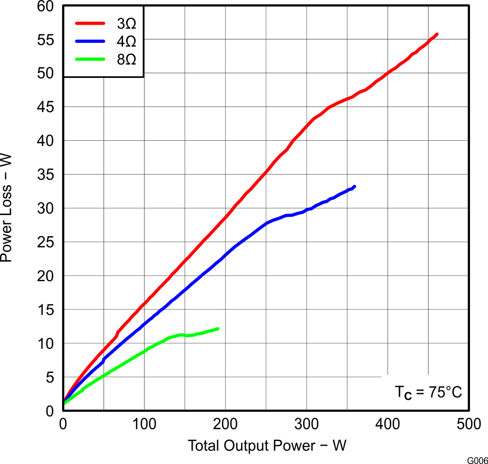 Figure 17. System Power Loss vs Output Power
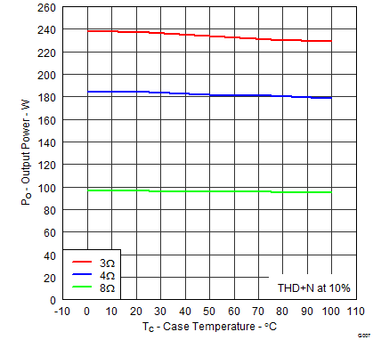 Figure 18. Output Power vs Temperature
10.2.2 Typical SE Configuration
See Figure 19 for application schematic. In this application, four single-ended PWM inputs are used with AD modulation from the PWM modulator such as the TAS5558. AD modulation scheme is defined as PWM(+) is opposite polarity from PWM(–). The single-ended (SE) output configuration is often used to drive four independent channels in one TAS5622A device.
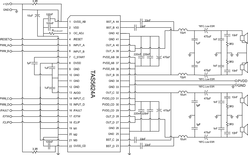 Figure 19. Typical (1N) SE Application
10.2.2.1 Design Requirements
Design Requirements lists the design parameters of Figure 19.
10.2.2.2 Detailed Design Procedure
Using Figure 16 as a guide, follow the design procedure in Detailed Design Procedure.
10.2.2.3 Application Curves
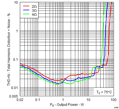
vs Output Power
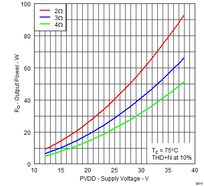
10.2.3 Typical PBTL Configuration
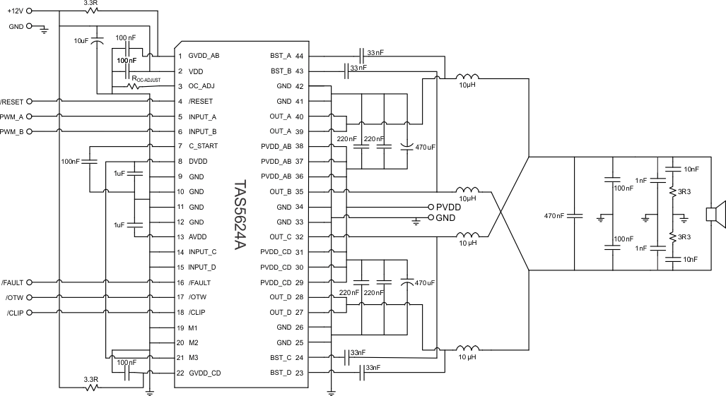 Figure 22. Typical Differential (2N) PBTL Application With AD Modulation Filter
10.2.3.1 Design Requirements
Design Requirements lists the design parameters of Figure 19.
10.2.3.2 Detailed Design Procedure
Using Figure 16 as a guide, follow the design procedure in Detailed Design Procedure.
10.2.3.3 Application Curves
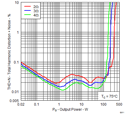
vs Output Power
