ZHCS928A May 2012 – January 2016 TAS5624A
PRODUCTION DATA.
- 1 特性
- 2 应用
- 3 说明
- 4 修订历史记录
- 5 Device Comparison Table
- 6 Pin Configuration and Functions
-
7 Specifications
- 7.1 Absolute Maximum Ratings
- 7.2 ESD Ratings
- 7.3 Recommended Operating Conditions
- 7.4 Thermal Information
- 7.5 Electrical Characteristics
- 7.6 Electrical Characteristics - Audio Specification Stereo (BTL)
- 7.7 Electrical Characteristics - Audio Specification 4 Channels (SE)
- 7.8 Electrical Characteristics - Audio Specification Mono (PBTL)
- 7.9 Typical Characteristics
- 8 Parameter Measurement Information
-
9 Detailed Description
- 9.1 Overview
- 9.2 Functional Block Diagrams
- 9.3
Feature Description
- 9.3.1 System Power-Up and Power-Down Sequence
- 9.3.2 Start-Up and Shutdown Ramp Sequence
- 9.3.3 Unused Output Channels
- 9.3.4 Device Protection System
- 9.3.5 Pin-to-Pin Short-Circuit Protection (PPSC)
- 9.3.6 Overtemperature Protection
- 9.3.7 Overtemperature Warning, OTW
- 9.3.8 Undervoltage Protection (UVP) and Power-On Reset (POR)
- 9.3.9 Error Reporting
- 9.3.10 Fault Handling
- 9.3.11 Device Reset
- 9.3.12 System Design Consideration
- 9.4 Device Functional Modes
- 10Application and Implementation
- 11Power Supply Recommendations
- 12Layout
- 13器件和文档支持
- 14机械、封装和可订购信息
7 Specifications
7.1 Absolute Maximum Ratings
over operating free-air temperature range unless otherwise noted(1)| MIN | MAX | UNIT | ||
|---|---|---|---|---|
| VDD to GND, GVDD_X(2) to GND | –0.3 | 13.2 | V | |
| PVDD_X(2) to GND, OUT_X to GND, BST_X to GVDD_X(2) | –0.3 | 50 | V | |
| BST_X to GND(3) | –0.3 | 62.5 | V | |
| DVDD to GND | –0.3 | 4.2 | V | |
| AVDD to GND | –0.3 | 8.5 | V | |
| OC_ADJ, M1, M2, M3, C_START, INPUT_X to GND | –0.3 | 4.2 | V | |
| RESET, FAULT, OTW, CLIP, to GND | –0.3 | 4.2 | V | |
| Maximum continuous sink current (FAULT, OTW, CLIP) | 9 | mA | ||
| Maximum operating junction temperature, TJ | 0 | 150 | °C | |
| Lead temperature | 260 | 260 | °C | |
| Storage temperature, Tstg | –40 | 150 | °C | |
(1) Stresses beyond those listed under Absolute Maximum Ratings may cause permanent damage to the device. These are stress ratings only, and functional operation of the device at these or any other conditions beyond those indicated under Recommended Operating Conditions is not implied. Exposure to absolute-maximum-rated conditions for extended periods may affect device reliability.
(2) GVDD_X and PVDD_X represents a full-bridge gate drive or power supply. GVDD_X is GVDD_AB or GVDD_CD, PVDD_X is PVDD_AB or PVDD_CD
(3) Maximum BST_X to GND voltage is the sum of maximum PVDD to GND and GVDD to GND voltages minus a diode drop.
7.2 ESD Ratings
| VALUE | UNIT | |||
|---|---|---|---|---|
| V(ESD) | Electrostatic discharge | Human-body model (HBM), per ANSI/ESDA/JEDEC JS-001(1) | ±2000 | V |
| Charged-device model (CDM), per JEDEC specification JESD22-C101(2) | ±500 | |||
(1) JEDEC document JEP155 states that 500-V HBM allows safe manufacturing with a standard ESD control process.
(2) JEDEC document JEP157 states that 250-V CDM allows safe manufacturing with a standard ESD control process.
7.3 Recommended Operating Conditions
| MIN | NOM | MAX | UNIT | ||||
|---|---|---|---|---|---|---|---|
| PVDD_X | Full-bridge supply | DC supply voltage | 12 | 36 | 38 | V | |
| GVDD_X | Supply for logic regulators and gate-drive circuitry | DC supply voltage | 10.8 | 12 | 13.2 | V | |
| VDD | Digital regulator supply voltage | DC supply voltage | 10.8 | 12 | 13.2 | V | |
| RL | Load impedance | BTL | Output filter: L = 10 uH, 1 µF. Output AD modulation, switching frequency > 350 kHz. |
2.5 | 4 | Ω | |
| SE | 1.5 | 3 | |||||
| PBTL | 1.5 | 2 | |||||
| LOUTPUT | Output filter inductance | Minimum inductance at overcurrent limit, including inductor tolerance, temperature and possible inductor saturation | 5 | μH | |||
| FPWM | PWM frame rate | 352 | 384 | 500 | kHz | ||
| CPVDD | PVDD close decoupling capacitors | 0.44 | 1 | μF | |||
| C_START | Start-up ramp capacitor | BTL and PBTL configuration | 100 | nF | |||
| SE and 1 × BTL+ 2 × SE configuration | 1 | μF | |||||
| ROC | Overcurrent programming resistor | Resistor tolerance = 5% | 24 | 33 | kΩ | ||
| ROC_LATCHED | Overcurrent programming resistor | Resistor tolerance = 5% | 47 | 62 | 68 | kΩ | |
| TJ | Junction temperature | 0 | 125 | °C | |||
7.4 Thermal Information
| THERMAL METRIC(1) | TAS5624A | UNIT | |
|---|---|---|---|
| DDV (HTSSOP) | |||
| 44 PINS | |||
| RθJA | Junction-to-ambient thermal resistance | 1.9 | °C/W |
| RθJC(top) | Junction-to-case (top) thermal resistance | 0.6 | °C/W |
| RθJB | Junction-to-board thermal resistance | 1.7 | °C/W |
| ψJT | Junction-to-top characterization parameter | 0.6 | °C/W |
| ψJB | Junction-to-board characterization parameter | 1.7 | °C/W |
| RθJC(bot) | Junction-to-case (bottom) thermal resistance | — | °C/W |
(1) For more information about traditional and new thermal metrics, see the Semiconductor and IC Package Thermal Metrics application report, SPRA953.
7.5 Electrical Characteristics
PVDD_X = 36 V, GVDD_X = 12 V, VDD = 12 V, TC (case temperature) = 75°C, fS = 384 kHz, unless otherwise specified.| PARAMETER | TEST CONDITIONS | MIN | TYP | MAX | UNIT | |
|---|---|---|---|---|---|---|
| INTERNAL VOLTAGE REGULATOR AND CURRENT CONSUMPTION | ||||||
| DVDD | Voltage regulator, only used as a reference node | VDD = 12 V | 3 | 3.3 | 3.6 | V |
| AVDD | Voltage regulator, only used as a reference node | VDD = 12 V | 7.8 | V | ||
| IVDD | VDD supply current | Operating, 50% duty cycle | 20 | mA | ||
| Idle, reset mode | 20 | |||||
| IGVDD_X | Gate-supply current per full-bridge | 50% duty cycle | 12 | mA | ||
| Reset mode | 3 | |||||
| IPVDD_X | Full-bridge idle current | 50% duty cycle without load | 15 | mA | ||
| RESET low | 1.9 | |||||
| VDD and GVDD_X at 0 V | 0.4 | |||||
| OUTPUT-STAGE MOSFETs | ||||||
| RDS(on), LS | Drain-to-source resistance, low-side (LS) | TJ = 25°C, excludes metallization resistance, GVDD = 12 V |
40 | mΩ | ||
| RDS(on), HS | Drain-to-source resistance, high-side (HS) | 40 | mΩ | |||
| I/O PROTECTION | ||||||
| Vuvp,GVDD | Undervoltage protection limit, GVDD_X | 8.5 | V | |||
| Vuvp,GVDD, hyst (1) | Undervoltage protection limit, GVDD_X | 0.7 | V | |||
| Vuvp,VDD | Undervoltage protection limit, VDD | 8.5 | V | |||
| Vuvp,VDD, hyst(1) | Undervoltage protection limit, VDD | 0.7 | V | |||
| Vuvp,PVDD | Undervoltage protection limit, PVDD_X | 8.5 | V | |||
| Vuvp,PVDD,hyst(1) | Undervoltage protection limit, PVDD_X | 0.7 | V | |||
| OTW(1) | Overtemperature warning | 115 | 125 | 135 | °C | |
| OTWhyst (1) | Temperature drop needed below OTW temperature for OTW to be inactive after OTW event. | 25 | °C | |||
| OTE(1) | Overtemperature error | 145 | 155 | 165 | °C | |
| OTE-OTWdifferential(1) | OTE-OTW differential | 30 | °C | |||
| OTEHYST (1) | A device reset is needed to clear FAULT after an OTE event | 25 | °C | |||
| OLPC | Overload protection counter | fPWM = 384 kHz | 2.6 | ms | ||
| IOC | Overcurrent limit protection | Resistor-programmable, nominal peak current in 1-Ω load, ROC = 24 kΩ |
15 | A | ||
| IOC_LATCHED | Overcurrent limit protection, latched | Resistor-programmable, nominal peak current in 1-Ω load, ROC = 62 kΩ |
15 | A | ||
| IOCT | Overcurrent response time | Time from application of short condition to Hi-Z of affected half-bridge | 150 | ns | ||
| IPD | Internal pulldown resistor at output of each half-bridge | Connected when RESET is active to provide bootstrap charge. Not used in SE mode. | 3 | mA | ||
| STATIC DIGITAL SPECIFICATIONS | ||||||
| VIH | High level input voltage | INPUT_X, M1, M2, M3, RESET | 1.9 | V | ||
| VIL | Low level input voltage | 0.8 | V | |||
| LEAKAGE | Input leakage current | 100 | μA | |||
| OTW / SHUTDOWN (FAULT) | ||||||
| RINT_PU | Internal pullup resistance, OTW, CLIP, FAULT to DVDD | 20 | 26 | 33 | kΩ | |
| VOH | High level output voltage | Internal pullup resistor | 3 | 3.3 | 3.6 | V |
| VOL | Low level output voltage | IO = 4 mA | 200 | 500 | mV | |
| FANOUT | Device fanout OTW, FAULT, CLIP | No external pullup | 30 | devices | ||
(1) Specified by design.
7.6 Electrical Characteristics – Audio Specification Stereo (BTL)
Audio performance is recorded as a chipset consisting of a TAS5558 8-Channel HD Compatible Audio Processor with ASRC and PWM Output (SLES273), PWM Processor (modulation index limited to 97.7%) and a TAS5624A power stage with PCB and system configurations in accordance with recommended guidelines.Audio frequency = 1 kHz, PVDD_X = 36 V, GVDD_X = 12 V, RL = 4 Ω, fS = 384 kHz, ROC = 24 kΩ, TC = 75°C, Output Filter: LDEM = 10 μH, CDEM = 1 µF, unless otherwise noted.
| PARAMETER | TEST CONDITIONS | MIN | TYP | MAX | UNIT | |
|---|---|---|---|---|---|---|
| PO | Power output per channel | RL = 3 Ω, 10% THD+N | 200 | W | ||
| RL = 4 Ω, 10% THD+N | 150 | |||||
| RL = 3 Ω, 1% THD+N | 160 | |||||
| RL = 4 Ω, 1% THD+N | 125 | |||||
| THD+N | Total harmonic distortion + noise | 1-W, 1-kHz signal | 0.025% | |||
| Vn | Output integrated noise | A-weighted, AES17 measuring filter | 180 | μV | ||
| VOS | Output offset voltage | No signal | 10 | 20 | mV | |
| SNR | Signal-to-noise ratio(1) | A-weighted, AES17 measuring filter | 105 | dB | ||
| DNR | Dynamic range | A-weighted, –60 dBFS (rel 1% THD+N) | 105 | dB | ||
| Pidle | Power dissipation due to idle losses (IPVDD_X) | PO = 0, channels switching(2) | 1 | W | ||
(1) SNR is calculated relative to 1% THD-N output level.
(2) Actual system idle losses also are affected by core losses of output inductors.
7.7 Electrical Characteristics – Audio Specification 4 Channels (SE)
Audio performance is recorded as a chipset consisting of a TASxxxx, PWM Processor (modulation index limited to 97.7%) and a TAS5624A power stage with PCB and system configurations in accordance with recommended guidelines.Audio frequency = 1 kHz, PVDD_X = 36 V, GVDD_X = 12V, RL = 4 Ω, fS = 384 kHz, R = 24 kΩ, TC = 75°C, Output Filter: LDEM = 10 μH, CDEM = 1 µF, CDCB = 470 µF, unless otherwise noted.
| PARAMETER | TEST CONDITIONS | MIN | TYP | MAX | UNIT | |
|---|---|---|---|---|---|---|
| PO | Power output per channel | RL = 3 Ω, 10% THD+N | 50 | W | ||
| RL = 3 Ω, 1% THD+N | 42 | |||||
| THD+N | Total harmonic distortion + noise | 1-W, 1-kHz signal | 0.025% | |||
| Vn | Output integrated noise | A-weighted, AES17 measuring filter | 180 | μV | ||
| SNR | Signal-to-noise ratio(1) | A-weighted, AES17 measuring filter | 102 | dB | ||
| DNR | Dynamic range | A-weighted, –60 dBFS (rel 1% THD+N) | 102 | dB | ||
| Pidle | Power dissipation due to Idle losses (IPVDD_X) | PO = 0, channels switching(2) | 1 | W | ||
(1) SNR is calculated relative to 1% THD-N output level.
(2) Actual system idle losses also are affected by core losses of output inductors.
7.8 Electrical Characteristics – Audio Specification Mono (PBTL)
Audio performance is recorded as a chipset consisting of a TASxxxx, PWM Processor (modulation index limited to 97.7%) and a TAS5624A power stage with PCB and system configurations in accordance with recommended guidelines.Audio frequency = 1 kHz, PVDD_X = 36 V, GVDD_X = 12 V, RL = 4 Ω, fS = 384 kHz, ROC = 24 kΩ, TC = 75°C, Output Filter: LDEM = 10 μH, CDEM = 1 μF, unless otherwise noted.
| PARAMETER | TEST CONDITIONS | MIN | TYP | MAX | UNIT | |
|---|---|---|---|---|---|---|
| PO | Power output per channel | RL = 1.5 Ω, 10%, THD+N | 400 | W | ||
| RL = 2 Ω, 10% THD+N | 300 | |||||
| RL = 4 Ω, 10% THD+N | 160 | |||||
| RL = 1.5 Ω, 1% THD+N | 320 | |||||
| RL = 2 Ω, 1% THD+N | 250 | |||||
| RL = 4 Ω, 1% THD+N | 130 | |||||
| THD+N | Total harmonic distortion + noise | 1-W, 1-kHz signal | 0.025% | |||
| Vn | Output integrated noise | A-weighted, AES17 measuring filter | 180 | μV | ||
| VOS | Output offset voltage | No signal | 10 | 20 | mV | |
| SNR | Signal-to-noise ratio(1) | A-weighted, AES17 measuring filter | 105 | dB | ||
| DNR | Dynamic range | A-weighted, –60 dBFS (rel 1% THD) | 105 | dB | ||
| Pidle | Power dissipation due to idle losses (IPVDD_X) | PO = 0, All channels switching(2) | 1 | W | ||
(1) SNR is calculated relative to 1% THD-N output level.
(2) Actual system idle losses are affected by core losses of output inductors.
7.9 Typical Characteristics
7.9.1 BTL Configuration
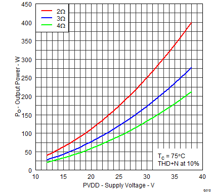
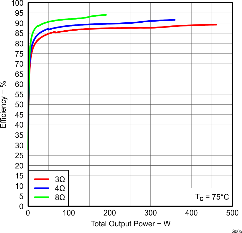
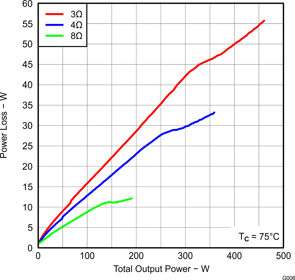
Measurement conditions are: 1 kHz, PVDD_X = 36 V, GVDD_X = 12 V, RL = 4 Ω, fS = 384 kHz, ROC = 24 kΩ, TC = 75°C, Output Filter: LDEM = 10 μH, CDEM = 1 µF, 20-Hz to 20-kHz BW (AES17 lowpass filter), unless otherwise noted.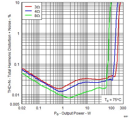
| 1 kHz |
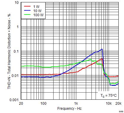
| 4 Ω |
vs Frequency
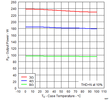
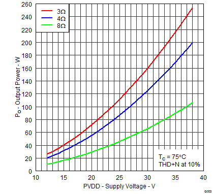
vs Distortion + Noise = 10%
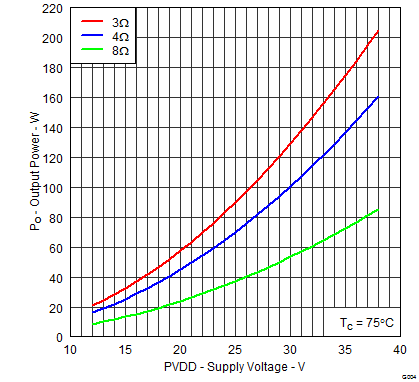
Distortion + Noise = 1%
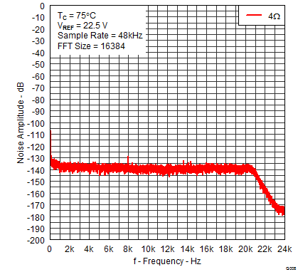
7.9.2 SE Configuration
Measurement conditions are: 1 kHz, PVDD_X = 36 V, GVDD_X = 12 V, RL = 4 Ω, fS = 384 kHz, ROC = 24 kΩ, TC = 75°C, Output Filter: LDEM = 10 μH, CDEM = 1 µF, CDCB = 470 µF, 20-Hz to 20-kHz BW (AES17 lowpass filter), unless otherwise noted.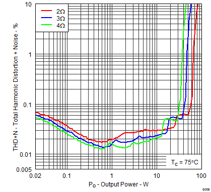
7.9.3 PBTL Configuration
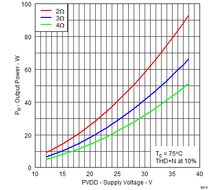
Measurement conditions are: 1 kHz, PVDD_X = 36 V, GVDD_X = 12 V, RL = 4 Ω, fS = 384 kHz, ROC = 24 kΩ, TC = 75°C, Output Filter: LDEM = 10 μH, CDEM = 1 µF, 20-Hz to 20-kHz BW (AES17 lowpass filter), unless otherwise noted.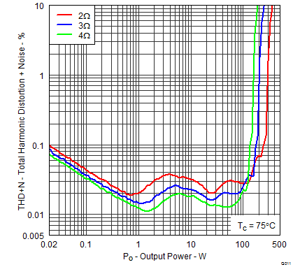
vs Output Power
