ZHCSH20 October 2017 TAS5634
PRODUCTION DATA.
- 1 特性
- 2 应用
- 3 说明
- 4 修订历史记录
- 5 Device Comparison
- 6 Pin Configuration and Functions
- 7 Specifications
-
8 Detailed Description
- 8.1 Overview
- 8.2 Functional Block Diagrams
- 8.3
Feature Description
- 8.3.1 Closed-Loop Architecture
- 8.3.2 Power Supplies
- 8.3.3 System Power-Up / Power-Down Sequence
- 8.3.4 Startup and Shutdown Ramp Sequence (C_START)
- 8.3.5 Device Protection System
- 8.3.6 Overload and Short Circuit Current Protection
- 8.3.7 DC Speaker Protection
- 8.3.8 Pin-To-Pin Short Circuit Protection (PPSC)
- 8.3.9 Overtemperature Protection
- 8.3.10 Overtemperature Warning, OTW
- 8.3.11 Undervoltage Protection (UVP) and Power-On Reset (POR)
- 8.3.12 Error Reporting
- 8.3.13 Fault Handling
- 8.3.14 System Design Consideration
- 8.4 Device Functional Modes
- 9 Application and Implementation
- 10Power Supply Recommendations
- 11Layout
- 12器件和文档支持
- 13机械、封装和可订购信息
11 Layout
11.1 Layout Guidelines
These requirements must be followed to achieve best performance and reliability and minimum ground bounce at rated output power of TAS5634.
11.1.1 PCB Material Recommendation
FR-4 Glass Epoxy material with 1oz. (35 μm) copper is recommended for use with the TAS5634. The use of this material can provide for higher power output, improved thermal performance and better EMI margin (due to lower PCB trace inductance).
11.1.2 PVDD Capacitor Recommendation
The large capacitors used in conjunction with each full-bridge, are referred to as the PVDD Capacitors. These capacitors should be selected for proper voltage margin and adequate capacitance to support the power requirements. In practice, with a well designed system power supply, 1000 μF, 75 V bulk capacitors should support most applications. The PVDD capacitors should be low ESR type because they are used in a circuit associated with high-speed switching.
11.1.3 Decoupling Capacitor Recommendation
To design an amplifier that has robust performance, passes regulatory requirements, and exhibits good audio performance, good quality decoupling capacitors should be used. In practice, X5R or better should be used in this application.
The voltage of the decoupling capacitors should be selected in accordance with good design practices. Temperature, ripple current, and voltage overshoot must be considered. This fact is particularly true in the selection of the close decoupling capacitor that is placed on the power supply to each half-bridge. It must withstand the voltage overshoot of the PWM switching, the heat generated by the amplifier during high power output, and the ripple current created by high power output. A minimum voltage rating of 100V is required for use with a 58 V power supply.
See the TAS5634EVM User's Guide for more details including layout and bill-of-material.
11.1.4 Circuit Component Requirements
A number of circuit components are critical to performance and reliability. They include LC filter inductors and capacitors, decoupling capacitors and the heatsink. The best detailed reference for these is the TAS5634EVM BOM in the user's guide, which includes components that meet all the following requirements.
- High frequency decoupling capacitors - small high frequency decoupling capacitors are placed next to the IC to control switching spikes and keep high frequency currents in a tight loop to achieve best performance and reliability and EMC. They must be high quality ceramic parts with material like X7R or X5R and voltage ratings at least 30% greater than PVDD, to minimize loss of capacitance caused by applied DC voltage. (Capacitors made of materials like Y5V or Z5U should never be used in decoupling circuits or audio circuits because their capacitance falls dramatically with applied DC and AC voltage, often to 20% of rated value or less.)
- Bulk decoupling capacitors - large bulk decoupling capacitors are placed as close as possible to the IC to stabilize the power supply at lower frequencies. They must be high quality aluminum parts with low ESR and ESL and voltage ratings at least 25% more than PVDD to handle power supply ripple currents and voltages.
- LC filter inductors - to maintain high efficiency, short circuit protection and low distortion, LC filter inductors must be linear to at least the OCP limit and must have low DC resistance and core losses. For SCP, minimum working inductance, including all variations of tolerance, temperature and current level, must be 5µH. Inductance variation of more than 1% over the output current range can cause increased distortion.
- LC filter capacitors - to maintain low distortion and reliable operation, LC filter capacitors must be linear to twice the peak output voltage. For reliability, capacitors must be rated to handle the audio current generated in them by the maximum expected audio output voltage at the highest audio frequency.
- Heatsink - The heatsink must be fabricated with the PowerPAD™ contact area spaced 1.0mm +/-0.01mm above mounting areas that contact the PCB surface. It must be supported mechanically at each end of the IC. This mounting ensures the correct pressure to provide good mechanical, thermal and electrical contact with TAS5634 PowerPAD™. The PowerPAD™ contact area must be bare and must be interfaced to the PowerPAD™ with a thin layer (about 1mil) of a thermal compound with high thermal conductivity.
11.1.5 Printed Circuit Board Requirements
PCB layout, audio performance, EMC and reliability are linked closely together, and solid grounding improves results in all these areas. The circuit produces high, fast-switching currents, and care must be taken to control current flow and minimize voltage spikes and ground bounce at IC ground pins. Critical components must be placed for best performance and PCB traces must be sized for the high audio currents that the IC circuit produces.
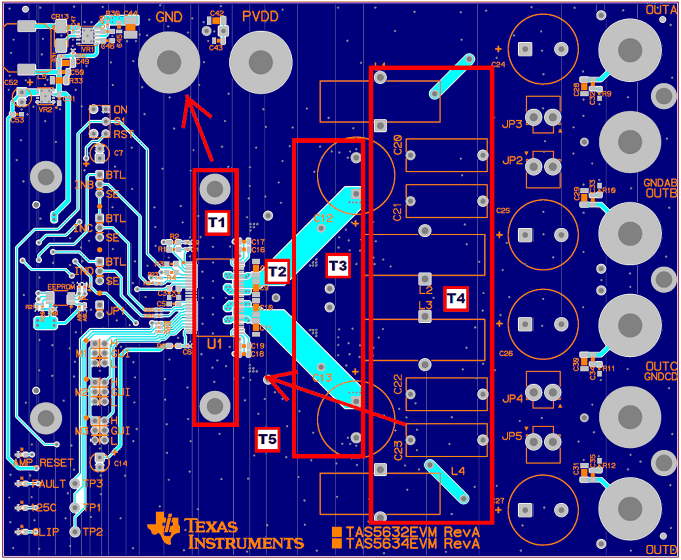
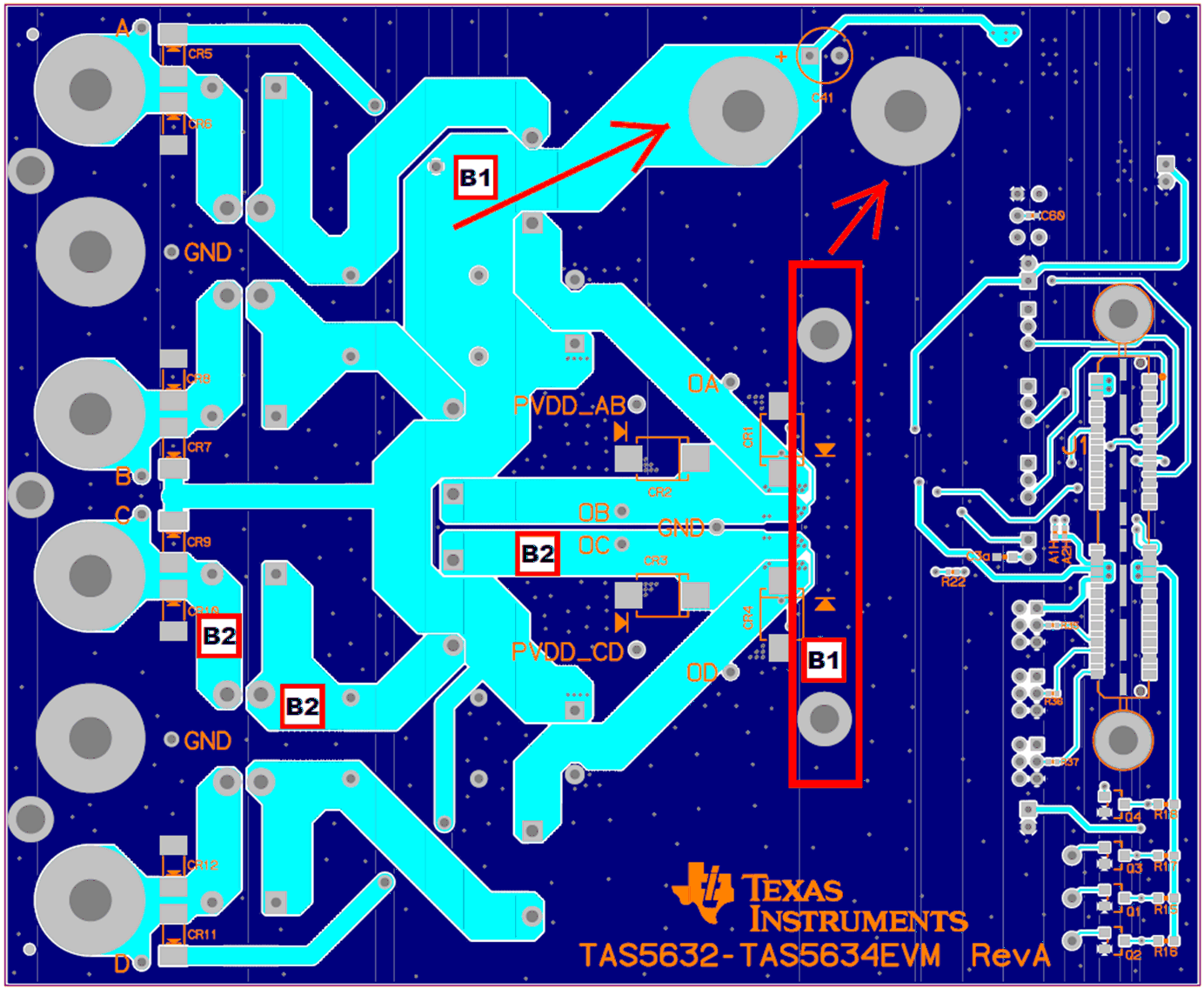
- Grounding - ground planes must be used to provide the lowest impedance and inductance for power and audio signal currents between the IC and its decoupling capacitors, LC filters and power supply connection. The area directly under the IC should be treated as central ground area for the device, and all IC grounds must be connected directly to that area. A matrix of vias must be used to connect that area to the ground plane. Ground planes can be interrupted by radial traces (traces pointing away from the IC), but they must never be interrupted by circular traces, which disconnect copper outside the circular trace from copper between it and the IC. Top and bottom areas that do not contain any power or signal traces should be flooded and connected with vias to the ground plane.
- Decoupling capacitors - high frequency decoupling capacitors must be located within 2mm of the IC and connected directly to PVDD and GND pins with solid traces. Vias must not be used to complete these connections, but several vias must be used at each capacitor location to connect top ground directly to the ground plane. Placement of bulk decoupling capacitors is less critical, but they still must be placed as close as possible to the IC with strong ground return paths. Typically the heatsink sets the distance.
- LC filters - LC filters must be placed as close as possible to the IC after the decoupling capacitors. The capacitors must have strong ground returns to the IC through top and bottom grounds for effective operation.
- PCB - PCB copper must be at least 1 ounce thickness. PVDD and output traces must be wide enough to carry expected average currents without excessive temperature rise. PWM input traces must be kept short and close together on the input side of the IC and must be shielded with ground flood to avoid interference from high power switching signals.
- Heat sink - The heatsink must be grounded well to the PCB near the IC, and a thin layer of highly conductive thermal compound (about 1mil) must be used to connect the heatsink to the PowerPAD™.
11.2 Layout Example

