ZHCSH20 October 2017 TAS5634
PRODUCTION DATA.
- 1 特性
- 2 应用
- 3 说明
- 4 修订历史记录
- 5 Device Comparison
- 6 Pin Configuration and Functions
- 7 Specifications
-
8 Detailed Description
- 8.1 Overview
- 8.2 Functional Block Diagrams
- 8.3
Feature Description
- 8.3.1 Closed-Loop Architecture
- 8.3.2 Power Supplies
- 8.3.3 System Power-Up / Power-Down Sequence
- 8.3.4 Startup and Shutdown Ramp Sequence (C_START)
- 8.3.5 Device Protection System
- 8.3.6 Overload and Short Circuit Current Protection
- 8.3.7 DC Speaker Protection
- 8.3.8 Pin-To-Pin Short Circuit Protection (PPSC)
- 8.3.9 Overtemperature Protection
- 8.3.10 Overtemperature Warning, OTW
- 8.3.11 Undervoltage Protection (UVP) and Power-On Reset (POR)
- 8.3.12 Error Reporting
- 8.3.13 Fault Handling
- 8.3.14 System Design Consideration
- 8.4 Device Functional Modes
- 9 Application and Implementation
- 10Power Supply Recommendations
- 11Layout
- 12器件和文档支持
- 13机械、封装和可订购信息
7 Specifications
7.1 Absolute Maximum Ratings
over operating free-air temperature range unless otherwise noted (1)| MIN | MAX | UNIT | ||
|---|---|---|---|---|
| VDD to GND, GVDD_X(3) to GND | –0.3 | 13.2 | V | |
| PVDD_X(3) to GND | –0.3 | 65 | V | |
| PVDD_X(3) to GND(2) (Less than 8ns transient) | -0.3 | 71 | V | |
| OUT_X to GND | -0.3 | 65 | V | |
| OUT_X to GND(2) (Less than 8ns transient) | -7 | 71 | V | |
| BST_X to OUT_X(3) | –0.3 | 13.2 | V | |
| DVDD to GND | –0.3 | 4.2 | V | |
| AVDD to GND | –0.3 | 8.5 | V | |
| OC_ADJ, M1, M2, M3, C_START, INPUT_X to GND | –0.3 | 4.2 | V | |
| RESET, FAULT, OTW, CLIP, to GND | –0.3 | 4.2 | V | |
| Maximum continuous sink current (FAULT, OTW, CLIP) | 9 | mA | ||
| Maximum operating junction temperature range, TJ | 0 | 150 | °C | |
| Storage temperature, Tstg | –40 | 150 | °C | |
7.2 ESD Ratings
| VALUE | UNIT | |||
|---|---|---|---|---|
| V(ESD) | Electrostatic discharge | Human-body model (HBM), per ANSI/ESDA/JEDEC JS-001(1) (3) | ±2000 | V |
| Electrostatic discharge | Charged-device model (CDM), per JEDEC specification JESD22-C101(2) (3) | ±500 | V | |
7.3 Recommended Operating Conditions
| MIN | TYP | MAX | UNIT | ||||
|---|---|---|---|---|---|---|---|
| PVDD_X | Full-bridge supply | DC supply voltage | 12 | 58 | 62 | V | |
| GVDD_X | Supply for logic regulators and gate-drive circuitry | DC supply voltage | 10.8 | 12 | 13.2 | V | |
| VDD | Digital regulator supply voltage | DC supply voltage | 10.8 | 12 | 13.2 | V | |
| RL | Load impedance | BTL | Output filter: L = 15 uH, 0.68 µF | 5 | 8 | Ω | |
| PBTL | 3 | 4 | |||||
| SE | 3 | 4 | |||||
| LOUTPUT | Output filter inductance | Minimum inductance at overcurrent limit, including inductor tolerance, temperature and possible inductor saturation | 7 | 15 | μH | ||
| fPWM | PWM frame rate | 352 | 384 | 500 | kHz | ||
| CPVDD | PVDD close decoupling capacitors | 0.44 | 1 | μF | |||
| C_START | Startup ramp capacitor | BTL and PBTL configuration | 330 | nF | |||
| SE and 1xBTL + 2xSE configuration | 1 | μF | |||||
| ROC | Over-current programming resistor, Resistor tolerance = 5% | 24 | 27 | 33 | kΩ | ||
| ROC_LATCHED | Over-current programming resistor, Resistor tolerance = 5% | 47 | 56 | 62 | kΩ | ||
| TJ | Junction temperature | 0 | 125 | °C | |||
7.4 Thermal Information
| THERMAL METRIC(1) | TAS5634 | UNIT | |
|---|---|---|---|
| DDV (HTSSOP) | |||
| 44 PINS | |||
| RθJA | Junction-to-ambient thermal resistance | 2.6 | °C/W |
| RθJC(top) | Junction-to-case (top) thermal resistance | 0.4 | °C/W |
| RθJB | Junction-to-board thermal resistance | 2.0 | °C/W |
| ψJT | Junction-to-top characterization parameter | 0.4 | °C/W |
| ψJB | Junction-to-board characterization parameter | 1.9 | °C/W |
| RθJC(bot) | Junction-to-case (bottom) thermal resistance | n/a | °C/W |
7.5 Audio Specification Stereo (BTL)
Audio performance is recorded as a chipset consisting of a TAS5548 PWM Processor (AD-mode, modulation index limited to 97.7%) and a TAS5634 power stage with PCB and system configurations in accordance with recommended guidelines. Audio frequency = 1 kHz, PVDD_X = 58 V, GVDD_X = 12 V, RL = 6 Ω, fS = 384 kHz, ROC = 30 kΩ, TC = 75°C, Output Filter: LDEM = 15 μH, CDEM = 680 nF, unless otherwise noted.| PARAMETER | TEST CONDITIONS | MIN | TYP | MAX | UNIT | |
|---|---|---|---|---|---|---|
| PO | Power output per channel | RL = 8 Ω, 10% THD+N | 230 | W | ||
| RL = 6 Ω, 10% THD+N Tc = 25°C | 300 | |||||
| RL = 6 Ω, 10% THD+N | 295 | |||||
| RL = 8 Ω, 1% THD+N | 180 | |||||
| RL = 6 Ω, 1% THD+N | 240 | |||||
| THD+N | Total harmonic distortion + noise | 1 W, 1 kHz signal | 0.025 | % | ||
| Vn | Output integrated noise | A-weighted, AES17 measuring filter, dither off, noise shaper off(1) | 215 | μV | ||
| VOS | Output offset voltage | No signal | 50 | mV | ||
| SNR | Signal-to-noise ratio(2) | A-weighted, AES17 measuring filter, noise shaper off | 105 | dB | ||
| DNR | Dynamic range | A-weighted, –60 dBFS (rel 1% THD+N), noise shaper on | 102 | dB | ||
| Pidle | Power dissipation due to Idle losses (IPVDD_X) | PO = 0, channels switching(3) | 8.6 | W | ||
7.6 Audio Specifications Mono (PBTL)
Audio performance is recorded as a chipset consisting of a TAS5548 PWM Processor (AD-mode, modulation index limited to 97.7%) and a TAS5634 power stage with PCB and system configurations in accordance with recommended guidelines. Audio frequency = 1 kHz, PVDD_X = 58 V, GVDD_X = 12 V, RL = 3 Ω, fS = 384 kHz, ROC = 30 kΩ, TC = 75°C, Output Filter: LDEM = 15 μH, CDEM = 680 nF, CDCB = 470 µF, unless otherwise noted.| PARAMETER | TEST CONDITIONS | MIN | TYP | MAX | UNIT | |
|---|---|---|---|---|---|---|
| PO | Power output per channel | RL = 4 Ω, 10% THD+N | 460 | W | ||
| RL = 3 Ω, 10% THD+N | 590 | |||||
| RL = 3 Ω, 10% THD+N, PVDD = 58.5V | 600 | |||||
| RL = 4 Ω, 1% THD+N | 365 | |||||
| RL = 3 Ω, 1% THD+N | 465 | |||||
| THD+N | Total harmonic distortion + noise | 1 W, 1 kHz signal | 0.04 | % | ||
| Vn | Output integrated noise | A-weighted, AES17 measuring filter, dither off, noise shaper off (1) | 214 | μV | ||
| VOS | Output offset voltage | No signal | 50 | mV | ||
| SNR | Signal-to-noise ratio(2) | A-weighted, AES17 measuring filter, noise shaper off | 105 | dB | ||
| DNR | Dynamic range | A-weighted, -60dBFS (rel 1% THD+N), noise shaper on | 102 | dB | ||
| Pidle | Power dissipation due to Idle losses (IPVDD_X) | PO = 0, channels switching(3) | 8.6 | W | ||
7.7 Audio Specification 4 Channels (SE)
Audio performance is recorded as a chipset consisting of a TAS5548 PWM Processor (AD-mode, modulation index limited to 97.7%) and a TAS5634 power stage with PCB and system configurations in accordance with recommended guidelines. Audio frequency = 1 kHz, PVDD_X = 58 V, GVDD_X = 12 V, RL = 3 Ω, fS = 384 kHz, ROC = 30 kΩ, TC = 75°C, Output Filter: LDEM = 15 μH, CDEM = 680 nF, CDCB = 470 µF, unless otherwise noted.| PARAMETER | TEST CONDITIONS | MIN | TYP | MAX | UNIT | |
|---|---|---|---|---|---|---|
| PO | Power output per channel | RL = 4 Ω, 10% THD+N | 110 | W | ||
| RL = 3 Ω, 10% THD+N Tc = 25°C | 150 | |||||
| RL = 3 Ω, 10% THD+N | 145 | |||||
| RL = 4 Ω, 1% THD+N | 90 | |||||
| RL = 3 Ω, 1% THD+N | 115 | |||||
| THD+N | Total harmonic distortion + noise | 1 W, 1 kHz signal | 0.05 | % | ||
| Vn | Output integrated noise | A-weighted, AES17 measuring filter, dither off, noise shaper off(1) | 145 | μV | ||
| SNR | Signal-to-noise ratio(2) | A-weighted, AES17 measuring filter, noise shaper off | 102 | dB | ||
| DNR | Dynamic range | A-weighted, –60 dBFS (rel 1% THD+N), noise shaper on | 102 | dB | ||
| Pidle | Power dissipation due to Idle losses (IPVDD_X) | PO = 0, channels switching(3) | 8.6 | W | ||
7.8 Electrical Characteristics
PVDD_X = 58 V, GVDD_X = 12 V, VDD = 12 V, TC (Case temperature) = 75°C, fS = 384 kHz, unless otherwise specified.| PARAMETER | TEST CONDITIONS | MIN | TYP | MAX | UNIT | |
|---|---|---|---|---|---|---|
| INTERNAL VOLTAGE REGULATOR AND CURRENT CONSUMPTION | ||||||
| DVDD | Voltage regulator, only used as a reference node | VDD = 12 V | 3.0 | 3.3 | 3.6 | V |
| AVDD | Voltage regulator, only used as a reference node | VDD = 12 V | 7.8 | V | ||
| IVDD | VDD supply current | Operating, 50% duty cycle | 23 | mA | ||
| Idle, reset mode | 23 | |||||
| IGVDD_X | Gate-supply current per full-bridge | 50% duty cycle | 22 | mA | ||
| Reset mode | 3 | |||||
| IPVDD_X | Full-bridge idle current | 50% duty cycle without load | 148 | mA | ||
| RESET low | 3.5 | |||||
| OUTPUT-STAGE MOSFETs | ||||||
| RDS(on), LS | Drain-to-source resistance, low side (LS) | TJ = 25°C, excludes metallization resistance, GVDD = 12 V |
80 | mΩ | ||
| RDS(on), HS | Drain-to-source resistance, high side (HS) | 80 | mΩ | |||
| I/O PROTECTION | ||||||
| Vuvp,GVDD | Undervoltage protection limit, GVDD_X | 8.5 | V | |||
| Vuvp,GVDD, hyst (1) | 0.7 | V | ||||
| Vuvp,VDD | Undervoltage protection limit, VDD | 8.5 | V | |||
| Vuvp,VDD, hyst (1) | 0.7 | V | ||||
| Vuvp,PVDD | Undervoltage protection limit, PVDD_X | 8.5 | V | |||
| Vuvp,PVDD,hyst (1) | 0.7 | V | ||||
| OTW(1) | Overtemperature warning | 115 | 125 | 135 | °C | |
| OTWhyst (1) | Temperature drop needed below OTW temperature for OTW to be inactive after OTW event. | 20 | °C | |||
| OTE(1) | Overtemperature error | 145 | 155 | 165 | °C | |
| OTE-OTWdifferential (1) | OTE-OTW differential | 30 | °C | |||
| OTEHYST (1) | A device reset is needed to clear FAULT after an OTE event | 20 | °C | |||
| OLPC | Overload protection counter | fPWM = 384 kHz | 2.6 | ms | ||
| IOC | Overcurrent limit protection | Resistor – programmable, nominal peak current in 1Ω load, ROC = 27 kΩ (Typ) | 14 | A | ||
| IOC_LATCHED | Overcurrent limit protection, latched | Resistor – programmable, nominal peak current in 1Ω load, ROC = 56 kΩ (Typ) | 14 | A | ||
| IDC_OC | Speaker DC protection limit | Resistor – programmable, ROC = 27 kΩ | 1.5 | A | ||
| IDC_OC_LATCHED | Speaker DC protection limit | Resistor – programmable, ROC = 56 kΩ | 1.5 | A | ||
| IOCT | Overcurrent response time | Time from application of short condition to Hi-Z of affected half bridge | 150 | ns | ||
| IPD | Internal pulldown resistor at output of each half bridge | Connected when RESET is active to provide bootstrap charge. Not used in SE mode. | 3 | mA | ||
| STATIC DIGITAL SPECIFICATIONS | ||||||
| VIH | High level input voltage | INPUT_X, M1, M2, M3, RESET | 1.9 | V | ||
| VIL | Low level input voltage | 0.8 | V | |||
| LEAKAGE | Input leakage current | 100 | μA | |||
| OTW / SHUTDOWN (FAULT) | ||||||
| RINT_PU | Internal pullup resistance, OTW, CLIP, FAULT to DVDD | 20 | 26 | 33 | kΩ | |
| VOH | High level output voltage | Internal pullup resistor | 3 | 3.3 | 3.6 | V |
| VOL | Low level output voltage | IO = 4mA | 200 | 500 | mV | |
| FANOUT | Device fanout OTW, FAULT, CLIP | No external pullup | 30 | devices | ||
7.9 Typical Characteristics
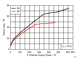
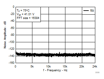
7.9.1 BTL Configuration
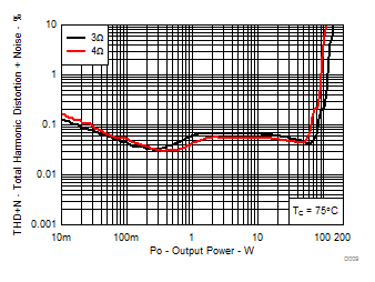
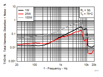
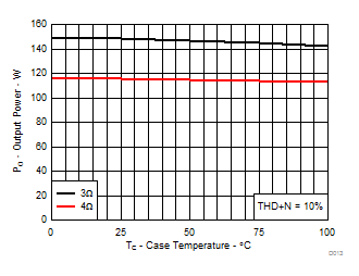
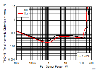
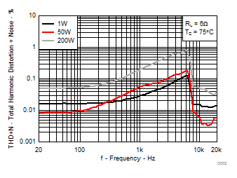
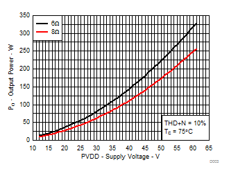
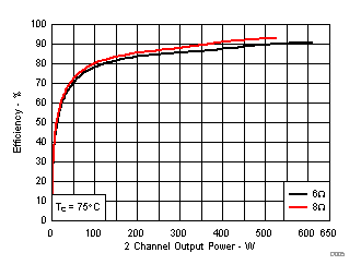
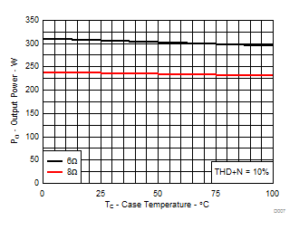
Measurement Conditions: TAS5548 PWM Processor (AD-mode, modulation index limited to 97.7%), Audio frequency = 1 kHz, PVDD_X = 58 V, GVDD_X = 12 V, RL = 6 Ω, fS = 384 kHz, ROC = 30 kΩ, TC = 75°C, Output Filter: LDEM = 15 μH, CDEM = 680 nF, 20 Hz to 20 kHz BW (AES17 low pass filter), unless otherwise noted.

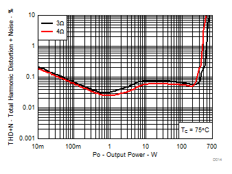
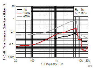
7.9.2 PBTL Configuration
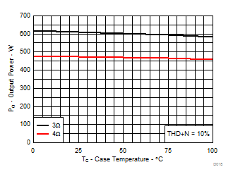
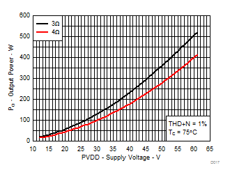
Measurement Conditions: TAS5548 PWM Processor (AD-mode, modulation index limited to 97.7%), Audio frequency = 1 kHz, PVDD_X = 58 V, GVDD_X = 12 V, RL = 3 Ω, fS = 384 kHz, ROC = 30 kΩ, TC = 75°C, Output Filter: LDEM = 15 μH, CDEM = 680 nF, CDCB = 470 µF, 20 Hz to 20 kHz BW (AES17 low pass filter), unless otherwise noted.

7.9.3 SE Configuration
Measurement Conditions: TAS5548 PWM Processor (AD-mode, modulation index limited to 97.7%), Audio frequency = 1 kHz, PVDD_X = 58 V, GVDD_X = 12 V, RL = 3 Ω, fS = 384 kHz, ROC = 30 kΩ, TC = 75°C, Output Filter: LDEM = 15 μH, CDEM = 680 nF, CDCB = 470 µF, 20 Hz to 20 kHz BW (AES17 low pass filter), unless otherwise noted.
