ZHCSET5B May 2015 – February 2016 TAS5720L , TAS5720M
PRODUCTION DATA.
- 1 特性
- 2 应用
- 3 说明
- 4 修订历史记录
- 5 Pin Configuration and Functions
- 6 Specifications
- 7 Detailed Description
- 8 Applications and Implementation
- 9 Power Supply Recommendations
- 10Layout
- 11器件和文档支持
- 12机械、封装和可订购信息
6 Specifications
6.1 Absolute Maximum Ratings
over operating free-air temperature range (unless otherwise noted)(1)| MIN | MAX | UNIT | ||
|---|---|---|---|---|
| Supply voltage(2) | PVDD, AVDD (TAS5720L) | –0.3 | 20 | V |
| PVDD, AVDD (TAS5720M) | –0.3 | 30 | ||
| DVDD | –0.3 | 4 | ||
| Digital input voltage | Digital inputs referenced to DVDD supply | –0.5 | VDVDD + 0.5 | V |
| Ambient operating temperature, TA | –25 | 85 | °C | |
| Storage temperature, Tstg | –40 | 125 | °C | |
6.2 ESD Ratings
| VALUE | UNIT | |||
|---|---|---|---|---|
| V(ESD) | Electrostatic discharge | Human body model (HBM), per ANSI/ESDA/JEDEC JS-001,(1) | ±4000 | V |
| Charged device model (CDM), per JEDEC specification JESD22-C101(2) | ±1500 | |||
6.3 Recommended Operating Conditions
over operating free-air temperature range (unless otherwise noted)| MIN | TYP | MAX | UNIT | |||
|---|---|---|---|---|---|---|
| PVDD/ AVDD |
Power supply voltage | TAS5720L | 4.5 | 16.5 | V | |
| TAS5720M | 4.5 | 26.4 | V | |||
| DVDD | Power supply voltage | 3 | 3.3 | 3.6 | V | |
| VIH(DR) | High-level digital input voltage | VDVDD | V | |||
| VIL(DR) | Low-level digital input voltage | 0 | V | |||
| RSPK | Minimum speaker load | 3.2 | Ω | |||
| TA | Operating free-air temperature | –25 | 85 | °C | ||
| TJ | Operating junction temperature | –25 | 150 | °C | ||
6.4 Thermal Information
| THERMAL METRIC(1) | TAS5720x | UNIT | |
|---|---|---|---|
| RSM (VQFN) | |||
| 32 PINS | |||
| RθJA | Junction-to-ambient thermal resistance | 37.3 | °C/W |
| RθJCtop | Junction-to-case (top) thermal resistance | 30.4 | °C/W |
| RθJB | Junction-to-board thermal resistance | 7.9 | °C/W |
| ψJT | Junction-to-top characterization parameter | 0.4 | °C/W |
| ψJB | Junction-to-board characterization parameter | 7.7 | °C/W |
| RθJCbot | Junction-to-case (bottom) thermal resistance | 2.5 | °C/W |
6.5 Electrical Characteristics
TA = 25ºC, V(PVDD) = 15 V, V(DVDD) = 3.3 V, RL = 4 Ω, fIN = 1 kHz, fs = 48 kHz, f(PWM) = 768 kHz, Gain = 20.7 dBV, SDZ = 1, Measured with an Audio Precision SYS-2722 High-Performance Audio Analyzer and using a 15-µH, 0.68-µF reconstruction filter at the device output.| PARAMETER | CONDITIONS | MIN | TYP | MAX | UNIT | |
|---|---|---|---|---|---|---|
| DIGITAL INPUT AND OUTPUT | ||||||
| VIH | High-level digital input logic voltage threshold | All digital pins | 70% VDVDD | |||
| VIL | Low-level digital input logic voltage threshold | All digital pins | 30% VDVDD | |||
| IIH | Input logic "high" leakage for digital inputs | All digital pins, excluding SDZ | 15 | µA | ||
| IIL | Input logic "low" leakage for digital inputs | All digital pins, excluding SDZ | –15 | µA | ||
| IIH(SDZ) | Input logic "high" leakage for SDZ inputs | SDZ | 1 | µA | ||
| IIL(SDZ) | Input logic "low" leakage for SDZ inputs | SDZ | –1 | µA | ||
| VOL | Output logic "low" for FAULTZ open drain Output | IOL = –2 mA | 10% VDVDD | |||
| CIN | Input capacitance for digital inputs | All digital pins | 5 | pF | ||
| MASTER CLOCK | ||||||
| D(MCLK) | Allowable MCLK duty cycle | 45% | 50% | 55% | ||
| f(MCLK) | MCLK input frequency | 25 | MHz | |||
| Supported single-speed MCLK frequencies | Values: 64, 128, 256, and 512 | 64 × fS | 512 × fS | |||
| Supported double-speed MCLK frequencies | Values: 64, 128, and 256 | 64 × fS | 256 × fS | |||
| SERIAL AUDIO PORT | ||||||
| D(BCLK) | Allowable BCLK duty cycle | 45% | 50% | 55% | ||
| f(BCLK) | BCLK input frequency | 25 | MHz | |||
| Supported single-speed BCLK frequencies | Values: 64, 128, 256, and 512 | 64 × fS | 512 × fS | |||
| Supported double-speed BCLK frequencies | Values: 64, 128, and 256 | 64 × fS | 256 × fS | |||
| fS | Supported single-speed input sample rates | Values: 44.1 and 48 | 44.1 | 48 | kHz | |
| Supported double-speed input sample rates | Values: 88.2 and 96 | 88.2 | 96 | kHz | ||
| I2C CONTROL PORT | ||||||
| CL(I2C) | Allowable load capacitance for each I2C Line | 400 | pF | |||
| fSCL | SCL frequency | No wait states | 400 | kHz | ||
| PROTECTION | ||||||
| OTE(THRESH) | Overtemperature error (OTE) threshold | 150 | °C | |||
| OTE(HYST) | Overtemperature error (OTE) hysteresis | 15 | °C | |||
| OCE(THRESH) | Overcurrent error (OCE) threshold | V(PVDD) = 16.5 V, TA = 25°C | 6 | A | ||
| DCE(THRESH) | DC error (DCE) threshold | V(PVDD) = 16.5 V, TA = 25°C | 2.6 | V | ||
| AMPLIFIER PERFORMANCE | ||||||
| POUT | Continuous average power | RL= 4 Ω, 10% THD+N, V(PVDD) = 7.2 V, fIN = 1 kHz |
6.6 | W | ||
| RL= 8 Ω, 10% THD+N, V(PVDD) = 7.2 V, fIN = 1 kHz |
3.7 | |||||
| RL= 4 Ω, 10% THD+N, V(PVDD) = 12 V, fIN = 1 kHz |
17.8 | |||||
| RL= 8 Ω, 10% THD+N, V(PVDD) = 12 V, fIN = 1 kHz |
10.1 | |||||
| RL= 4 Ω, 10% THD+N, V(PVDD) = 15 V, fIN = 1 kHz, TA= 60°C |
27.4 | |||||
| RL= 8 Ω, 10% THD+N, V(PVDD) = 15 V, fIN = 1 kHz |
15.8 | |||||
| RL= 4 Ω, 10% THD+N, V(PVDD) = 19 V, fIN = 1 kHz |
27 | |||||
| RL= 8 Ω, 10% THD+N, V(PVDD) = 19 V, fIN = 1 kHz |
25.3 | |||||
| RL= 4 Ω, 10% THD+N, V(PVDD) = 24 V, fIN = 1 kHz |
22.1 | |||||
| RL= 8 Ω, 10% THD+N, V(PVDD) = 24 V, fIN = 1 kHz |
39.8 | |||||
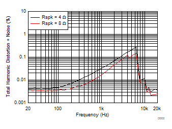
| THD+N | Total harmonic distortion plus noise | RL= 4 Ω,V(PVDD) = 7.2 V, POUT = 1 W, fIN = 1 kHz |
0.033% | |||
| RL= 8 Ω,V(PVDD) = 7.2 V, POUT = 1 W, fIN = 1 kHz |
0.015% | |||||
| RL= 4 Ω, V(PVDD)= 12 V, POUT = 1 W, fIN = 1 kHz |
0.03% | |||||
| RL= 8 Ω, V(PVDD)= 12 V, POUT = 1 W, 20 Hz ≤ fIN ≤ 20 kHz |
0.013v | |||||
| RL= 4 Ω, V(PVDD) = 15 V, POUT = 1 W, 20 Hz ≤ fIN≤ 20 kHz |
0.028% | |||||
| RL= 8 Ω, V(PVDD) = 15 V, POUT = 1 W, 20 Hz ≤ fIN≤ 20 kHz |
0.012% | |||||
| RL= 4 Ω, V(PVDD) = 19 V, POUT = 1 W, 20 Hz ≤ fIN ≤ 20 kHz |
0.026% | |||||
| RL= 8 Ω, V(PVDD) = 19 V, POUT = 1 W, 20 Hz ≤ fIN ≤ 20 kHz |
0.013% | |||||
| RL= 4 Ω, V(PVDD) = 24 V, POUT = 1 W, 20 Hz ≤ fIN ≤ 20 kHz |
0.026% | |||||
| RL= 8 Ω, V(PVDD) = 24 V, POUT = 1 W, 20 Hz ≤ fIN ≤ 20 kHz |
0.016% | |||||
| PEFF | Power efficiency | RL= 8 Ω, V(PVDD) = 12 V, POUT = 9 W | 91% | |||
| RL= 8 Ω, V(PVDD) = 12 V, POUT = 9 W; fPWM = 384 kHz | 90% | |||||
| RL= 8 Ω, V(PVDD) = 24 V, POUT = 40 W | 90% | |||||
| VN | Integrated noise floor voltage | A-Weighted,RL= 8 Ω, Gain = 20.7 dBV | 50 | µVrms | ||
| φCC | Channel-to-channel phase shift | Output phase shift between multiple devices from 20 Hz to 20 kHz. Across all sample frequencies and SAIF operating modes. | 0.2 | deg | ||
| A(RIPPLE) | Frequency response | Maximum deviation above or below passband gain. | ±0.15 | dB | ||
| -3 dB Output Cutoff Frequency | 0.47 × fS | Hz | ||||
| AV(00) | Amplifier analog gain(1) | ANALOG_GAIN[1:0] register bits set to "00" | 19.2 | dBV | ||
| AV(01) | ANALOG_GAIN[1:0] register bits set to "01" | 20.7 | ||||
| AV(10) | ANALOG_GAIN[1:0] register bits set to "10" | 23.5 | ||||
| AV(11) | ANALOG_GAIN[1:0] register bits set to "11" | 26.3 | ||||
| AV(ERROR) | Amplifier analog gain error | ±0.15 | dB | |||
| VOS | DC output offset voltage | Measured between OUTP and OUTN | 1.5 | mV | ||
| KCP | Click-pop performance | –60 | dBV | |||
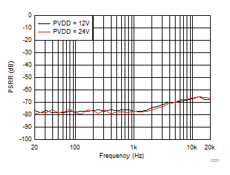
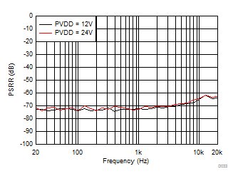
| PSRR | Power supply rejection ratio | DC, 5.5 V ≤ V(PVDD) ≤ 26.4 V | 87 | dB | ||
| AC, V(PVDD)= 16.5 V + 100 mVP-P, f(RIPPLE) from 20 Hz to 10 kHz | 53 | |||||
| AC, V(PVDD)= 16.5 V + 100 mVP-P, f(RIPPLE) from 10 Hz to 20 kHz | 50 | |||||
| RDS(on)FET | Power stage FET on-resistance | TA = 25°C | 120 | mΩ | ||
| RDS(on)TOT | Power stage total on-resistance (FET+bond+package) | TA = 25°C | 150 | mΩ | ||
| IPK | Peak output current | TA = 25°C | 5 | A | ||
| f(HP) | –3 dB high-pass filter corner frequency | f = 44.1 kHz | 3.675 | Hz | ||
| f = 48 kHz | 4 | |||||
| f = 88.2 kHz | 7.35 | |||||
| f = 96 kHz | 8 | |||||
| f(PWM) | PWM switching frequency | Values: 6, 8, 10, 12, 14, 16, 20, and 24 | 6 | 24 | fS | |
6.6 Timing Requirements
| MIN | NOM | MAX | UNIT | |||
|---|---|---|---|---|---|---|
| tACTIVE | Shutdown to Active Time | From deassertion of SDZ (both pin and I2C register bit) until the Class-D amplifier begins switching. | 25 | ms | ||
| tWAKE | Wake Time | From the deassertion of SLEEP until the Class-D amplifier starts switching. | 1 | |||
| tSLEEP | Sleep Time | From the assertion of SLEEP until the Class-D amplifier stops switching. | tvrmp + 1 | |||
| tMUTE | Play to Mute Time | From the assertion of MUTE mode until the volume has ramped to the minimum. | tvrmp | |||
| tPLAY | Un-Mute to Play Time | From the deassertion of MUTE until the volume has returned to its current setting. | tvrmp | |||
| tSD | Active to Shutdown Time | From the assertion of SDZ (pin or I2C register bit) until the Class-D amplifier stops switching. | tvrmp + 1 | |||
| SERIAL AUDIO PORT | ||||||
| tH_L | Time high and low, BCLK, LRCLK, SDIN inputs | 10 | ns | |||
| tSU
tHLD |
Setup and hold time. LRCLK, SDIN input to BCLK edge. | Input tRISE ≤ 1 ns, input tFALL ≤ 1 ns | 5 | ns | ||
| Input tRISE ≤ 4 ns, input tFALL ≤ 4 ns | 8 | |||||
| Input tRISE ≤ 8 ns, input tFALL ≤ 8 ns | 12 | |||||
| tRISE | Rise-time BCLK, LRCLK, SDIN inputs | 8 | ns | |||
| tFALL | Fall-time BCLK, LRCLK, SDIN inputs | 8 | ||||
| I2C CONTROL PORT | ||||||
| tBUS | Bus free time between start and stop conditions | 1.3 | µs | |||
| tHOLD1(I2C) | Hold Time, SCL to SDA | 80 | ns | |||
| tHOLD2(I2C) | Hold Time, start condition to SCL | 0.6 | µs | |||
| tSTART(I2C) | I2C Startup Time after DVDD Power On Reset | 12 | ms | |||
| tRISE(I2C) | Rise Time, SCL and SDA | 300 | ns | |||
| tFALL(I2C) | Fall Time, SCL and SDA | 300 | ns | |||
| tSU1(I2C) | Setup, SDA to SCL | 100 | ns | |||
| tSU2(I2C) | Setup, SCL to start condition | 0.6 | µs | |||
| tSU3(I2C) | Setup, SCL to stop condition | 0.6 | µs | |||
| tW(H) | Required pulse duration, SCL "HIGH" | 0.6 | µs | |||
| tW(L) | Required pulse duration, SCL "LOW" | 1.3 | µs | |||
| PROTECTION | ||||||
| tFAULTZ | Amplifier fault time-out period | DC detect error | 650 | ms | ||
| OTE or OCE fault | 1.3 | s | ||||
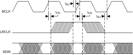 Figure 1. SAIF Timing
 Figure 2. SCL and SDA Timing
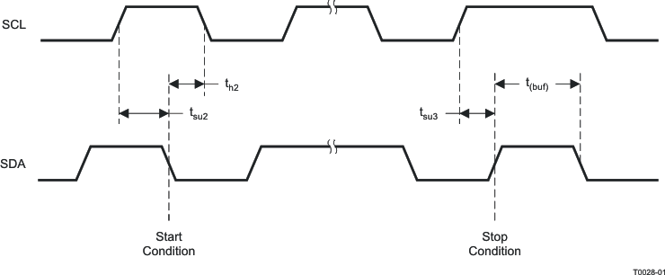 Figure 3. Start and Stop Conditions Timing
When SDZ is deasserted (and the device is not in sleep mode), the amplifier begins to switch after a period of tACTIVE. At this point, the volume ramps from –100 dB to the programmed digital volume control (DVC) setting at a rate of 0.5 dB every eight sample periods. Ramping the volume prevents audible artifacts that can occur if discontinuous volume changes are applied while audio is being played back. This period, tVRMP, depends on the DVC setting and sample rate. Typical values for tVRMP for a DVC of 0 dB are shown in Timing Requirements. Figure 4 illustrates mode timing.
The time to enter or exit sleep or mute and the time to enter shudown are dominated by tVRMP. Table 1 lists the timing parameters based on tVRMP.
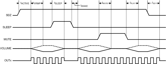 Figure 4. Mode Timing
Table 1. Typical DVC Ramp Times
| SAMPLE RATE (kHZ) |
RAMP TIMES (tVRAMP) FROM –100 dB to 0 dB (ms) |
|---|---|
| 44.1 | 36.3 |
| 48 | 33.3 |
| 88.2 | 18.1 |
| 96 | 16.7 |
6.7 Typical Characteristics
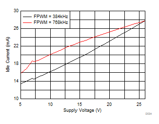
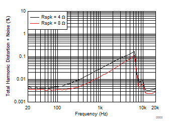
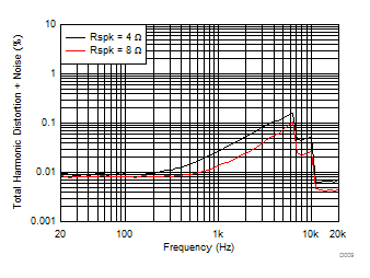
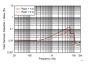
TA = 25ºC, V(PVDD) = 15 V, V(DVDD) = 3.3 V, RL = 4 Ω, fIN = 1 kHz, fs = 48 kHz, f(PWM) = 768 kHz, Gain = 20.7 dBV, SDZ = 1, Measured with an Audio Precision SYS-2722 High-Performance Audio Analyzer and using a 15-µH, 0.68-µF reconstruction filter at the device output.
| V(PVDD) = 12 V | POUT = 1 W | f(PWM) = 384 kHz |
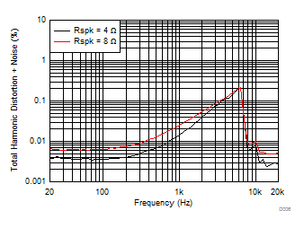
| V(PVDD) = 15 V | POUT = 1 W | f(PWM) = 384 kHz |
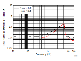
| V(PVDD) = 19 V | POUT = 1 W | f(PWM) = 384 kHz |
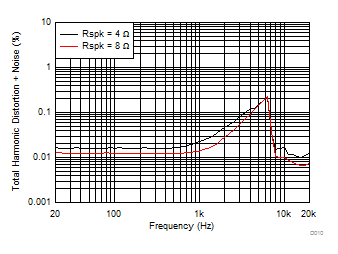
| V(PVDD) = 24 V | POUT = 1 W | f(PWM) = 384 kHz |
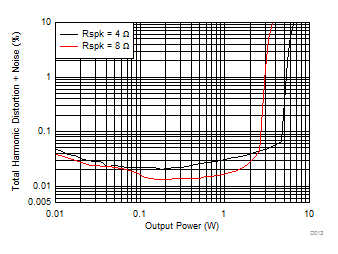
| V(PVDD) = 7.2 V | f(PWM) = 384 kHz |
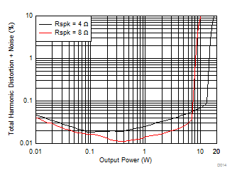
| V(PVDD) = 12 V | f(PWM) = 384 kHz |
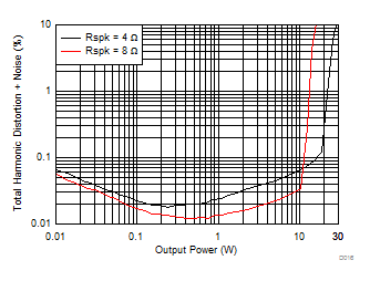
| V(PVDD) = 15 V | f(PWM) = 384 kHz |
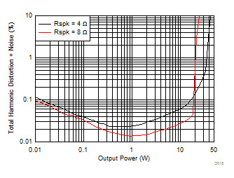
| V(PVDD) = 19 V | f(PWM) = 384 kHz |

| V(PVDD) = 24 V | f(PWM) = 384 kHz |
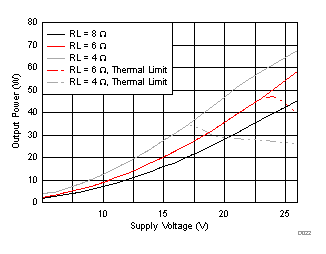
| Analog Gain = Setting 11 | f(PWM) = 384 kHz |
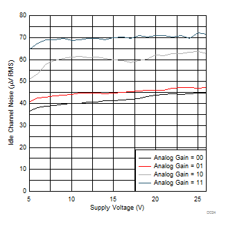
| f(PWM) = 384 kHz |
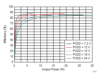
| RL = 4 Ω | f(PWM) = 384 kHz |
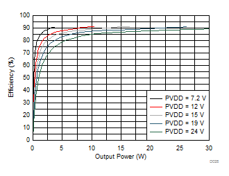
| RL = 8 Ω | f(PWM) = 384 kHz |
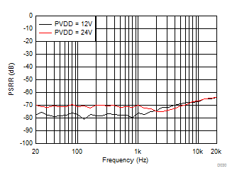
| f(PWM) = 384 kHz |
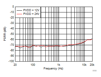
| f(PWM) = 384 kHz |

| V(PVDD) = 7.2 V | POUT = 1 W |
| V(PVDD) = 12 V | POUT = 1 W |

| V(PVDD) = 15 V | POUT = 1 W |
| V(PVDD) = 19 V | POUT = 1 W |
| V(PVDD) = 24 V | POUT = 1 W |
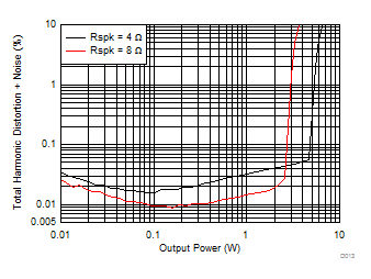
| V(PVDD) = 7.2 V |
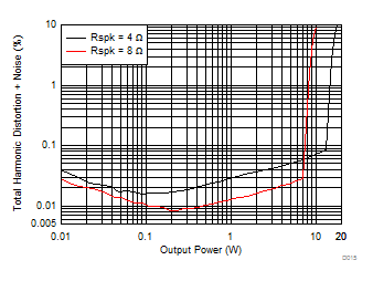
| V(PVDD) = 12 V |
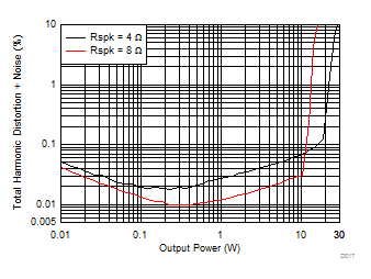
| V(PVDD) = 15 V |
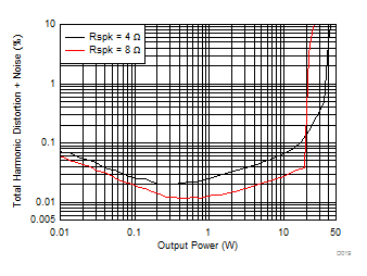
| V(PVDD) = 19 V |
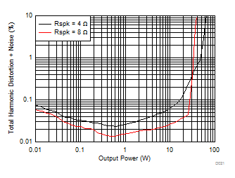
| V(PVDD) = 24 V | Gain = 20.7 dBV |
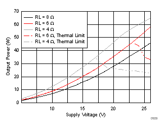
| Analog Gain = Setting 11 |
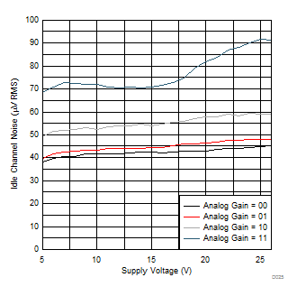
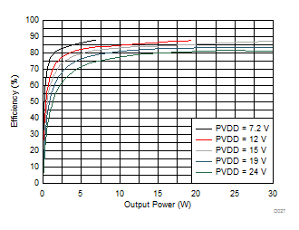
| RL = 4 Ω |
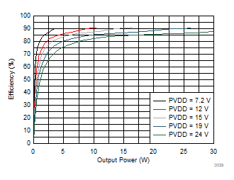
| RL = 8 Ω |
