ZHCSI79B March   2016  – May 2018 TAS5751M

PRODUCTION DATA.  

  1. 特性
  2. 应用
  3. 说明
    1.     Device Images
      1.      功率与 PVDD 间的关系
      2.      简化框图
  4. 修订历史记录
  5. Pin Configuration and Functions
    1.     Pin Functions
  6. Specifications
    1. 6.1  Absolute Maximum Ratings
    2. 6.2  ESD Ratings
    3. 6.3  Recommended Operating Conditions
    4. 6.4  Thermal Characteristics
    5. 6.5  Electrical Characteristics
    6. 6.6  Speaker Amplifier Characteristics
    7. 6.7  Protection Characteristics
    8. 6.8  Master Clock Characteristics
    9. 6.9  I²C Interface Timing Requirements
    10. 6.10 Serial Audio Port Timing Requirements
    11. 6.11 Typical Characteristics
      1. 6.11.1 Typical Characteristics - Stereo BTL Mode
      2. 6.11.2 Typical Characteristics - Mono PBTL Mode
  7. Detailed Description
    1. 7.1 Overview
    2. 7.2 Functional Block Diagram
    3. 7.3 Audio Signal Processing Overview
    4. 7.4 Feature Description
      1. 7.4.1 Clock, Autodetection, and PLL
      2. 7.4.2 PWM Section
      3. 7.4.3 PWM Level Meter
      4. 7.4.4 Automatic Gain Limiter (AGL)
      5. 7.4.5 Headphone/Line Amplifier
      6. 7.4.6 Fault Indication
      7. 7.4.7 SSTIMER Pin Functionality
      8. 7.4.8 Device Protection System
        1. 7.4.8.1 Overcurrent (OC) Protection With Current Limiting
        2. 7.4.8.2 Overtemperature Protection
        3. 7.4.8.3 Undervoltage Protection (UVP) and Power-On Reset (POR)
    5. 7.5 Device Functional Modes
      1. 7.5.1 Serial Audio Port Operating Modes
      2. 7.5.2 Communication Port Operating Modes
      3. 7.5.3 Speaker Amplifier Modes
        1. 7.5.3.1 Stereo Mode
        2. 7.5.3.2 Mono Mode
    6. 7.6 Programming
      1. 7.6.1 I²C Serial Control Interface
        1. 7.6.1.1 General I²C Operation
        2. 7.6.1.2 I²C Slave Address
          1. 7.6.1.2.1 I²C Device Address Change Procedure
        3. 7.6.1.3 Single- and Multiple-Byte Transfers
        4. 7.6.1.4 Single-Byte Write
        5. 7.6.1.5 Multiple-Byte Write
        6. 7.6.1.6 Single-Byte Read
        7. 7.6.1.7 Multiple-Byte Read
      2. 7.6.2 Serial Interface Control and Timing
        1. 7.6.2.1 Serial Data Interface
        2. 7.6.2.2 I²S Timing
        3. 7.6.2.3 Left-Justified
        4. 7.6.2.4 Right-Justified
      3. 7.6.3 26-Bit 3.23 Number Format
    7. 7.7 Register Maps
      1. 7.7.1 Register Summary
      2. 7.7.2 Detailed Register Descriptions
        1. 7.7.2.1  Clock Control Register (0x00)
        2. 7.7.2.2  Device ID Register (0x01)
        3. 7.7.2.3  Error Status Register (0x02)
        4. 7.7.2.4  System Control Register 1 (0x03)
        5. 7.7.2.5  Serial Data Interface Register (0x04)
        6. 7.7.2.6  System Control Register 2 (0x05)
        7. 7.7.2.7  Soft Mute Register (0x06)
        8. 7.7.2.8  Volume Registers (0x07, 0x08, 0x09)
        9. 7.7.2.9  Volume Configuration Register (0x0E)
        10. 7.7.2.10 Modulation Limit Register (0x10)
        11. 7.7.2.11 Interchannel Delay Registers (0x11, 0x12, 0x13, and 0x14)
        12. 7.7.2.12 PWM Shutdown Group Register (0x19)
        13. 7.7.2.13 Start/Stop Period Register (0x1A)
        14. 7.7.2.14 Oscillator Trim Register (0x1B)
        15. 7.7.2.15 BKND_ERR Register (0x1C)
        16. 7.7.2.16 Input Multiplexer Register (0x20)
        17. 7.7.2.17 PWM Output MUX Register (0x25)
        18. 7.7.2.18 AGL Control Register (0x46)
        19. 7.7.2.19 PWM Switching Rate Control Register (0x4F)
        20. 7.7.2.20 Bank Switch and EQ Control (0x50)
  8. Application and Implementation
    1. 8.1 Application Information
      1. 8.1.1 External Component Selection Criteria
        1. 8.1.1.1 Component Selection Impact on Board Layout, Component Placement, and Trace Routing
        2. 8.1.1.2 Amplifier Output Filtering
    2. 8.2 Typical Applications
      1. 8.2.1 Stereo Bridge Tied Load Application
        1. 8.2.1.1 Design Requirements
        2. 8.2.1.2 Detailed Design Procedure
          1. 8.2.1.2.1 Component Selection and Hardware Connections
          2. 8.2.1.2.2 Control and Software Integration
          3. 8.2.1.2.3 I²C Pullup Resistors
          4. 8.2.1.2.4 Digital I/O Connectivity
          5. 8.2.1.2.5 Recommended Startup and Shutdown Procedures
            1. 8.2.1.2.5.1 Start-Up Sequence
            2. 8.2.1.2.5.2 Normal Operation
            3. 8.2.1.2.5.3 Shutdown Sequence
            4. 8.2.1.2.5.4 Power-Down Sequence
        3. 8.2.1.3 Application Performance Plots
      2. 8.2.2 Mono Parallel Bridge Tied Load Application
        1. 8.2.2.1 Design Requirements
        2. 8.2.2.2 Detailed Design Procedure
        3. 8.2.2.3 Application Performance Plots
  9. Power Supply Recommendations
  10. 10Layout
    1. 10.1 Layout Guidelines
      1. 10.1.1 Decoupling Capacitors
      2. 10.1.2 Thermal Performance and Grounding
    2. 10.2 Layout Example
  11. 11器件和文档支持
    1. 11.1 商标
    2. 11.2 静电放电警告
    3. 11.3 术语表
  12. 12机械、封装和可订购信息

封装选项

机械数据 (封装 | 引脚)
散热焊盘机械数据 (封装 | 引脚)
订购信息

I²S Timing

I²S timing uses LRCK to define when the data being transmitted is for the left channel and when the data is for the right channel. LRCK is low for the left channel and high for the right channel. A bit clock running at 32 × fS, 48 × fS, or 64 × fS is used to clock in the data. A delay of one bit clock exists from the time the LRCK signal changes state to the first bit of data on the data lines. The data is written MSB-first and is valid on the rising edge of bit clock. The DAP masks unused trailing data bit positions.
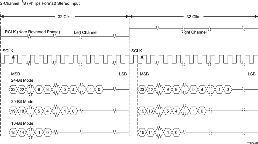
TAS5751M t0034-01.gif

NOTE:

All data presented in two's-complement form with MSB first.
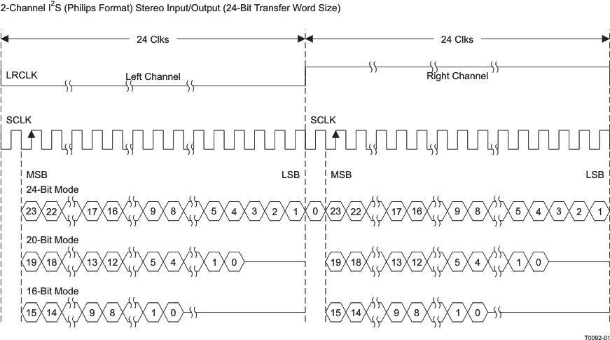
Figure 55. I²S 64-fS Format
TAS5751M t0092-01.gif

NOTE:

All data presented in two's-complement form with MSB first.
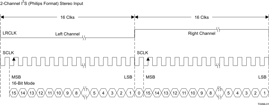
Figure 56. I²S 48-fS Format
TAS5751M t0266-01_los549.gif

NOTE:

All data presented in two's-complement form with MSB first.
Figure 57. I²S 32-fS Format