ZHCSH30C August 2017 – April 2018 TAS5755M
PRODUCTION DATA.
- 1 特性
- 2 应用
- 3 说明
- 4 修订历史记录
- 5 Device Comparison Table
- 6 Pin Configuration and Functions
-
7 Specifications
- 7.1 Absolute Maximum Ratings
- 7.2 ESD Ratings
- 7.3 Recommended Operating Conditions
- 7.4 Thermal Information
- 7.5 PWM Operation at Recommended Operating Conditions
- 7.6 DC Electrical Characteristics
- 7.7 AC Electrical Characteristics (BTL, PBTL)
- 7.8 Electrical Characteristics - PLL External Filter Components
- 7.9 Electrical Characteristic - I2C Serial Control Port Operation
- 7.10 Timing Requirements - PLL Input Parameters
- 7.11 Timing Requirements - Serial Audio Ports Slave Mode
- 7.12 Timing Requirements - I2C Serial Control Port Operation
- 7.13 Timing Requirements - Reset (RESET)
- 7.14 Typical Characteristics
- 8 Parameter Measurement Information
-
9 Detailed Description
- 9.1 Overview
- 9.2 Functional Block Diagrams
- 9.3
Feature Description
- 9.3.1 Power Supply
- 9.3.2 I2C Address Selection and Fault Output
- 9.3.3 Single-Filter PBTL Mode
- 9.3.4 Device Protection System
- 9.3.5 SSTIMER Functionality
- 9.3.6 Clock, Autodetection, and PLL
- 9.3.7 PWM Section
- 9.3.8 2.1-Mode Support
- 9.3.9 I2C Compatible Serial Control Interface
- 9.3.10 Audio Serial Interface
- 9.3.11 Dynamic Range Control (DRC)
- 9.4 Device Functional Modes
- 9.5 Programming
- 9.6
Register Maps
- 9.6.1 Register Map Summary
- 9.6.2
Register Maps
- 9.6.2.1 Clock Control Register (0x00)
- 9.6.2.2 Device ID Register (0x01)
- 9.6.2.3 Error Status Register (0x02)
- 9.6.2.4 System Control Register 1 (0x03)
- 9.6.2.5 Serial Data Interface Register (0x04)
- 9.6.2.6 System Control Register 2 (0x05)
- 9.6.2.7 Soft Mute Register (0x06)
- 9.6.2.8 Volume Registers (0x07, 0x08, 0x09, 0x0A)
- 9.6.2.9 Volume Configuration Register (0x0E)
- 9.6.2.10 Modulation Limit Register (0x10)
- 9.6.2.11 Interchannel Delay Registers (0x11, 0x12, 0x13, and 0x14)
- 9.6.2.12 PWM Shutdown Group Register (0x19)
- 9.6.2.13 Start/Stop Period Register (0x1A)
- 9.6.2.14 Oscillator Trim Register (0x1B)
- 9.6.2.15 BKND_ERR Register (0x1C)
- 9.6.2.16 Input Multiplexer Register (0x20)
- 9.6.2.17 Channel 4 Source Select Register (0x21)
- 9.6.2.18 PWM Output Mux Register (0x25)
- 9.6.2.19 DRC Control Register (0x46)
- 9.6.2.20 Bank Switch and EQ Control Register (0x50)
-
10Application and Implementation
- 10.1 Application Information
- 10.2
Typical Applications
- 10.2.1 Stereo Bridge Tied Load Application
- 10.2.2 Mono Parallel Bridge Tied Load Application
- 10.2.3 2.1 Application
- 11Power Supply Recommendations
- 12Layout
- 13器件和文档支持
9.3.10.1 I2S Timing
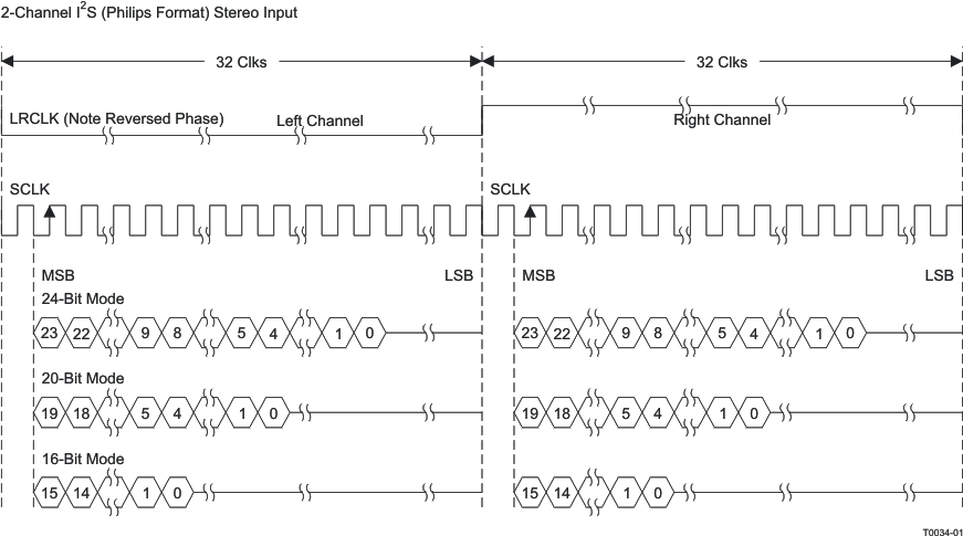
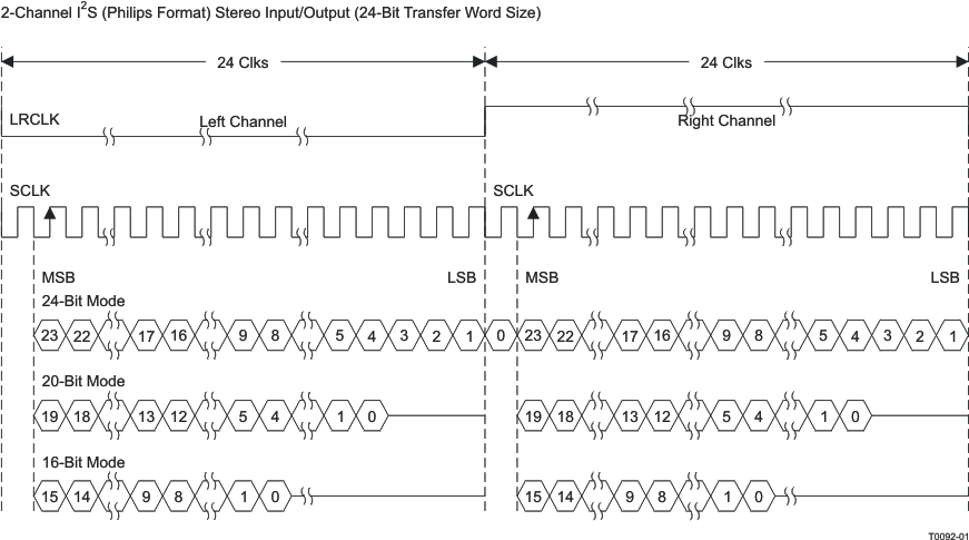
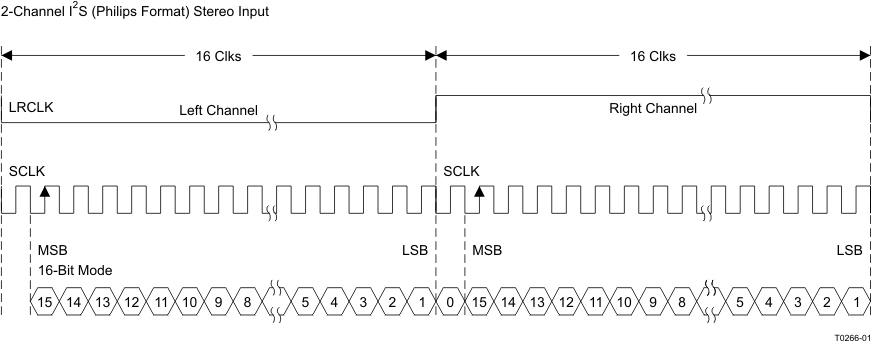
I2S timing uses LRCLK to define when the data being transmitted is for the left channel and when it is for the right channel. LRCLK is low for the left channel and high for the right channel. A bit clock running at 32, 48, or 64 × fS is used to clock in the data. There is a delay of one bit clock from the time the LRCLK signal changes state to the first bit of data on the data lines. The data is written MSB-first and is valid on the rising edge of bit clock. The DAP masks unused trailing data bit positions.

NOTE:
All data presented in 2s-complement form with MSB first.
NOTE:
All data presented in 2s-complement form with MSB first.
NOTE:
All data presented in 2s-complement form with MSB first.