ZHCSH30C August 2017 – April 2018 TAS5755M
PRODUCTION DATA.
- 1 特性
- 2 应用
- 3 说明
- 4 修订历史记录
- 5 Device Comparison Table
- 6 Pin Configuration and Functions
-
7 Specifications
- 7.1 Absolute Maximum Ratings
- 7.2 ESD Ratings
- 7.3 Recommended Operating Conditions
- 7.4 Thermal Information
- 7.5 PWM Operation at Recommended Operating Conditions
- 7.6 DC Electrical Characteristics
- 7.7 AC Electrical Characteristics (BTL, PBTL)
- 7.8 Electrical Characteristics - PLL External Filter Components
- 7.9 Electrical Characteristic - I2C Serial Control Port Operation
- 7.10 Timing Requirements - PLL Input Parameters
- 7.11 Timing Requirements - Serial Audio Ports Slave Mode
- 7.12 Timing Requirements - I2C Serial Control Port Operation
- 7.13 Timing Requirements - Reset (RESET)
- 7.14 Typical Characteristics
- 8 Parameter Measurement Information
-
9 Detailed Description
- 9.1 Overview
- 9.2 Functional Block Diagrams
- 9.3
Feature Description
- 9.3.1 Power Supply
- 9.3.2 I2C Address Selection and Fault Output
- 9.3.3 Single-Filter PBTL Mode
- 9.3.4 Device Protection System
- 9.3.5 SSTIMER Functionality
- 9.3.6 Clock, Autodetection, and PLL
- 9.3.7 PWM Section
- 9.3.8 2.1-Mode Support
- 9.3.9 I2C Compatible Serial Control Interface
- 9.3.10 Audio Serial Interface
- 9.3.11 Dynamic Range Control (DRC)
- 9.4 Device Functional Modes
- 9.5 Programming
- 9.6
Register Maps
- 9.6.1 Register Map Summary
- 9.6.2
Register Maps
- 9.6.2.1 Clock Control Register (0x00)
- 9.6.2.2 Device ID Register (0x01)
- 9.6.2.3 Error Status Register (0x02)
- 9.6.2.4 System Control Register 1 (0x03)
- 9.6.2.5 Serial Data Interface Register (0x04)
- 9.6.2.6 System Control Register 2 (0x05)
- 9.6.2.7 Soft Mute Register (0x06)
- 9.6.2.8 Volume Registers (0x07, 0x08, 0x09, 0x0A)
- 9.6.2.9 Volume Configuration Register (0x0E)
- 9.6.2.10 Modulation Limit Register (0x10)
- 9.6.2.11 Interchannel Delay Registers (0x11, 0x12, 0x13, and 0x14)
- 9.6.2.12 PWM Shutdown Group Register (0x19)
- 9.6.2.13 Start/Stop Period Register (0x1A)
- 9.6.2.14 Oscillator Trim Register (0x1B)
- 9.6.2.15 BKND_ERR Register (0x1C)
- 9.6.2.16 Input Multiplexer Register (0x20)
- 9.6.2.17 Channel 4 Source Select Register (0x21)
- 9.6.2.18 PWM Output Mux Register (0x25)
- 9.6.2.19 DRC Control Register (0x46)
- 9.6.2.20 Bank Switch and EQ Control Register (0x50)
-
10Application and Implementation
- 10.1 Application Information
- 10.2
Typical Applications
- 10.2.1 Stereo Bridge Tied Load Application
- 10.2.2 Mono Parallel Bridge Tied Load Application
- 10.2.3 2.1 Application
- 11Power Supply Recommendations
- 12Layout
- 13器件和文档支持
9.4.2 Mono PBTL Mode
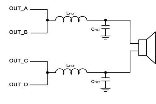
When this mode of operation is used, the two stereo outputs of the device are placed in parallel one with another to increase the power sourcing capabilities of the device. The TAS5755M supports parallel BTL (PBTL) mode with OUT_A/OUT_B (and OUT_C/OUT_D) connected before the LC filter.
The merging of the two output channels in this device can be done before the inductor portion of the output filter. This is called Single-Filter PBTL, and this mono operation is shown in Figure 58. More information about this can be found in Single-Filter PBTL Mode section.
 Figure 58. Pre-Filter PBTL
On the input side of the TAS5755M device, the input signal to the mono amplifier can be selected from a mix, left or right frame from an I2S, LJ, or RJ signal. The routing of the audio data which is presented on the SPK_OUTx outputs must be configured with the PWM Output Mux Register (0x25) and PWM Shutdown Group Register (0x19).
Refer to the Mono Parallel Bridge Tied Load Application section for more details of the correct PBTL output connection of the TAS5755M.