ZHCSH30C August 2017 – April 2018 TAS5755M
PRODUCTION DATA.
- 1 特性
- 2 应用
- 3 说明
- 4 修订历史记录
- 5 Device Comparison Table
- 6 Pin Configuration and Functions
-
7 Specifications
- 7.1 Absolute Maximum Ratings
- 7.2 ESD Ratings
- 7.3 Recommended Operating Conditions
- 7.4 Thermal Information
- 7.5 PWM Operation at Recommended Operating Conditions
- 7.6 DC Electrical Characteristics
- 7.7 AC Electrical Characteristics (BTL, PBTL)
- 7.8 Electrical Characteristics - PLL External Filter Components
- 7.9 Electrical Characteristic - I2C Serial Control Port Operation
- 7.10 Timing Requirements - PLL Input Parameters
- 7.11 Timing Requirements - Serial Audio Ports Slave Mode
- 7.12 Timing Requirements - I2C Serial Control Port Operation
- 7.13 Timing Requirements - Reset (RESET)
- 7.14 Typical Characteristics
- 8 Parameter Measurement Information
-
9 Detailed Description
- 9.1 Overview
- 9.2 Functional Block Diagrams
- 9.3
Feature Description
- 9.3.1 Power Supply
- 9.3.2 I2C Address Selection and Fault Output
- 9.3.3 Single-Filter PBTL Mode
- 9.3.4 Device Protection System
- 9.3.5 SSTIMER Functionality
- 9.3.6 Clock, Autodetection, and PLL
- 9.3.7 PWM Section
- 9.3.8 2.1-Mode Support
- 9.3.9 I2C Compatible Serial Control Interface
- 9.3.10 Audio Serial Interface
- 9.3.11 Dynamic Range Control (DRC)
- 9.4 Device Functional Modes
- 9.5 Programming
- 9.6
Register Maps
- 9.6.1 Register Map Summary
- 9.6.2
Register Maps
- 9.6.2.1 Clock Control Register (0x00)
- 9.6.2.2 Device ID Register (0x01)
- 9.6.2.3 Error Status Register (0x02)
- 9.6.2.4 System Control Register 1 (0x03)
- 9.6.2.5 Serial Data Interface Register (0x04)
- 9.6.2.6 System Control Register 2 (0x05)
- 9.6.2.7 Soft Mute Register (0x06)
- 9.6.2.8 Volume Registers (0x07, 0x08, 0x09, 0x0A)
- 9.6.2.9 Volume Configuration Register (0x0E)
- 9.6.2.10 Modulation Limit Register (0x10)
- 9.6.2.11 Interchannel Delay Registers (0x11, 0x12, 0x13, and 0x14)
- 9.6.2.12 PWM Shutdown Group Register (0x19)
- 9.6.2.13 Start/Stop Period Register (0x1A)
- 9.6.2.14 Oscillator Trim Register (0x1B)
- 9.6.2.15 BKND_ERR Register (0x1C)
- 9.6.2.16 Input Multiplexer Register (0x20)
- 9.6.2.17 Channel 4 Source Select Register (0x21)
- 9.6.2.18 PWM Output Mux Register (0x25)
- 9.6.2.19 DRC Control Register (0x46)
- 9.6.2.20 Bank Switch and EQ Control Register (0x50)
-
10Application and Implementation
- 10.1 Application Information
- 10.2
Typical Applications
- 10.2.1 Stereo Bridge Tied Load Application
- 10.2.2 Mono Parallel Bridge Tied Load Application
- 10.2.3 2.1 Application
- 11Power Supply Recommendations
- 12Layout
- 13器件和文档支持
9.5.2 26-Bit 3.23 Number Format
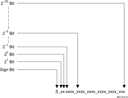
All mixer gain coefficients are 26-bit coefficients using a 3.23 number format. Numbers formatted as 3.23 numbers means that there are 3 bits to the left of the binary point and 23 bits to the right of the binary point. This is shown in Figure 65.
 Figure 65. 3.23 Format
The decimal value of a 3.23 format number can be found by following the weighting shown in Figure 65. If the most significant bit is logic 0, the number is a positive number, and the weighting shown yields the correct number. If the most significant bit is a logic 1, then the number is a negative number. In this case every bit must be inverted, a 1 added to the result, and then the weighting shown in Figure 66 applied to obtain the magnitude of the negative number.
 Figure 66. Conversion Weighting Factors — 3.23 Format To Floating Point
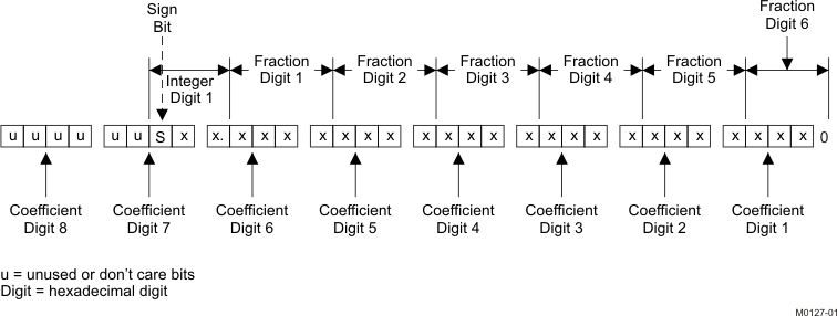
Gain coefficients, entered via the I2C bus, must be entered as 32-bit binary numbers. The format of the 32-bit number (4-byte or 8-digit hexadecimal number) is shown in Figure 67.
 Figure 67. Alignment of 3.23 Coefficient in 32-Bit I2C Word
Table 1. Sample Calculation for 3.23 Format
| db | LINEAR | DECIMAL | HEX (3.23 Format) |
|---|---|---|---|
| 0 | 1 | 8,388,608 | 80 0000 |
| 5 | 1.77 | 14,917,288 | 00E3 9EA8 |
| –5 | 0.56 | 4,717,260 | 0047 FACC |
| X | L = 10(X/20) | D = 8,388,608 × L | H = dec2hex (D, 8) |
Table 2. Sample Calculation for 9.17 Format
| db | LINEAR | DECIMAL | HEX (9.17 Format) |
|---|---|---|---|
| 0 | 1 | 131,072 | 2 0000 |
| 5 | 1.77 | 231,997 | 3 8A3D |
| –5 | 0.56 | 73,400 | 1 1EB8 |
| X | L = 10(X/20) | D = 131,072 × L | H = dec2hex (D, 8) |