ZHCSBA9C July 2013 – November 2017 TAS5760LD
PRODUCTION DATA.
- 1 特性
- 2 应用
- 3 说明
- 4 修订历史记录
- 5 Pin Configuration and Functions
-
6 Specifications
- 6.1 Absolute Maximum Ratings
- 6.2 ESD Ratings
- 6.3 Recommended Operating Conditions
- 6.4 Thermal Information
- 6.5 Digital I/O Pins
- 6.6 Master Clock
- 6.7 Serial Audio Port
- 6.8 Protection Circuitry
- 6.9 Speaker Amplifier in All Modes
- 6.10 Speaker Amplifier in Stereo Bridge-Tied Load (BTL) Mode
- 6.11 Speaker Amplifier in Mono Parallel Bridge-Tied Load (PBTL) Mode
- 6.12 Headphone Amplifier and Line Driver
- 6.13 I²C Control Port
- 6.14 Typical Idle, Mute, Shutdown, Operational Power Consumption
- 6.15 Typical Speaker Amplifier Performance Characteristics (Stereo BTL Mode)
- 6.16 Typical Performance Characteristics (Mono PBTL Mode)
- 7 Parameter Measurement Information
-
8 Detailed Description
- 8.1 Overview
- 8.2 Functional Block Diagram
- 8.3 Feature Description
- 8.4
Device Functional Modes
- 8.4.1
Hardware Control Mode
- 8.4.1.1 Speaker Amplifier Shut Down (SPK_SD Pin)
- 8.4.1.2 Serial Audio Port in Hardware Control Mode
- 8.4.1.3 Soft Clipper Control (SFT_CLIP Pin)
- 8.4.1.4 Speaker Amplifier Switching Frequency Select (FREQ/SDA Pin)
- 8.4.1.5 Parallel Bridge Tied Load Mode Select (PBTL/SCL Pin)
- 8.4.1.6 Speaker Amplifier Sleep Enable (SPK_SLEEP/ADR Pin)
- 8.4.1.7 Speaker Amplifier Gain Select (SPK_GAIN [1:0] Pins)
- 8.4.1.8 Considerations for Setting the Speaker Amplifier Gain Structure
- 8.4.2 Software Control Mode
- 8.4.1
Hardware Control Mode
- 8.5
Register Maps
- 8.5.1 Control Port Registers - Quick Reference
- 8.5.2
Control Port Registers - Detailed Description
- 8.5.2.1 Device Identification Register (0x00)
- 8.5.2.2 Power Control Register (0x01)
- 8.5.2.3 Digital Control Register (0x02)
- 8.5.2.4 Volume Control Configuration Register (0x03)
- 8.5.2.5 Left Channel Volume Control Register (0x04)
- 8.5.2.6 Right Channel Volume Control Register (0x05)
- 8.5.2.7 Analog Control Register (0x06)
- 8.5.2.8 Reserved Register (0x07)
- 8.5.2.9 Fault Configuration and Error Status Register (0x08)
- 8.5.2.10 Reserved Controls (9 / 0x09) - (15 / 0x0F)
- 8.5.2.11 Digital Clipper Control 2 Register (0x10)
- 8.5.2.12 Digital Clipper Control 1 Register (0x11)
-
9 Application and Implementation
- 9.1 Application Information
- 9.2
Typical Applications
- 9.2.1
Stereo BTL Using Software Control
- 9.2.1.1 Design Requirements
- 9.2.1.2
Detailed Design Procedure
- 9.2.1.2.1 Startup Procedures- Software Control Mode
- 9.2.1.2.2 Shutdown Procedures- Software Control Mode
- 9.2.1.2.3 Component Selection and Hardware Connections
- 9.2.1.2.4 Recommended Startup and Shutdown Procedures
- 9.2.1.2.5
Headphone and Line Driver Amplifier
- 9.2.1.2.5.1 Charge-Pump Flying Capacitor and DR_VSS Capacitor
- 9.2.1.2.5.2 Decoupling Capacitors
- 9.2.1.2.5.3 Gain-Setting Resistor Ranges
- 9.2.1.2.5.4 Using the Line Driver Amplifier in the TAS5760LD as a Second-Order Filter
- 9.2.1.2.5.5 External Undervoltage Detection
- 9.2.1.2.5.6 Input-Blocking Capacitors
- 9.2.1.2.6 Gain-Setting Resistors
- 9.2.1.3 Application Curves
- 9.2.2 Stereo BTL Using Hardware Control
- 9.2.3 Mono PBTL Using Software Control
- 9.2.4 Mono PBTL Using Hardware Control
- 9.2.1
Stereo BTL Using Software Control
- 10Power Supply Recommendations
- 11Layout
- 12器件和文档支持
- 13机械、封装和可订购信息
8.4.1.3 Soft Clipper Control (SFT_CLIP Pin)
The TAS5760LD has a soft clipper that can be used to clip the output voltage level below the supply rail. When this circuit is active, the amplifier operates as if it was powered by a lower supply voltage, and thereby enters into clipping sooner than if the circuit was not active. The result is clipping behavior very similar to that of clipping at the PVDD rail, in contrast to the digital clipper behavior which occurs in the oversampled domain of the digital path. The point at which clipping begins is controlled by a resistor divider from GVDD_REG to ground, which sets the voltage at the SFT_CLIP pin. The precision of the threshold at which clipping occurs is dependent upon the voltage level at the SFT_CLIP pin. Because of this, increasing the precision of the resistors used to create the voltage divider, or using an external reference will increase the precision of the point at which the device enters into clipping. To ensure stability, and soften the edges of the clipping event, a capacitor should be connected from pin SFT_CLIP to ground.
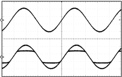
 Figure 41. Soft Clipper Example Wave Form
To move the output stage into clipping, the soft clipper circuit limits the duty cycle of the output PWM pulses to a fixed maximum value. After filtering this limit applied to the duty cycle resembles a clipping event at a voltage below that of the PVDD level. The peak voltage level attainable when the soft clipper circuit is active, called VP in the example below, is approximately 4 times the voltage at the SFT_CLIP pin, noted as VSFT_CLIP. This voltage can be used to calculate the maximum output power for a given maximum input voltage and speaker impedance, as shown in the equation below.

Where:
RS is the total series resistance including RDS(on), and output filter resistance.
RL is the load resistance.
VP is the peak amplitude achievable when the soft clipper circuit is active (As mentioned previously, VP = [4 x VSFT_CLIP], provided that [4 x VSFT_CLIP] < PVDD.)
POUT (10%THD) ≈ 1.25 × POUT (unclipped)
If the PVDD level is below (4 x VSFT_CLIP) clipping will occur due to clipping at PVDD before the clipping due to the soft clipper circuit becomes active.
Table 4. Soft Clipper Example
| PVDD [V] | SFT_CLIP Pin Voltage [V] | Resistor to GND [kΩ] | Resistor to GVDD [kΩ] | Output Voltage [Vrms] |
|---|---|---|---|---|
| 12 | GVDD | (Open) | 0 | 10.33 |
| 12 | 2.25 | 24 | 51 | 9.00 |
| 12 | 1.5 | 18 | 68 | 6.30 |