ZHCSBA9C July 2013 – November 2017 TAS5760LD
PRODUCTION DATA.
- 1 特性
- 2 应用
- 3 说明
- 4 修订历史记录
- 5 Pin Configuration and Functions
-
6 Specifications
- 6.1 Absolute Maximum Ratings
- 6.2 ESD Ratings
- 6.3 Recommended Operating Conditions
- 6.4 Thermal Information
- 6.5 Digital I/O Pins
- 6.6 Master Clock
- 6.7 Serial Audio Port
- 6.8 Protection Circuitry
- 6.9 Speaker Amplifier in All Modes
- 6.10 Speaker Amplifier in Stereo Bridge-Tied Load (BTL) Mode
- 6.11 Speaker Amplifier in Mono Parallel Bridge-Tied Load (PBTL) Mode
- 6.12 Headphone Amplifier and Line Driver
- 6.13 I²C Control Port
- 6.14 Typical Idle, Mute, Shutdown, Operational Power Consumption
- 6.15 Typical Speaker Amplifier Performance Characteristics (Stereo BTL Mode)
- 6.16 Typical Performance Characteristics (Mono PBTL Mode)
- 7 Parameter Measurement Information
-
8 Detailed Description
- 8.1 Overview
- 8.2 Functional Block Diagram
- 8.3 Feature Description
- 8.4
Device Functional Modes
- 8.4.1
Hardware Control Mode
- 8.4.1.1 Speaker Amplifier Shut Down (SPK_SD Pin)
- 8.4.1.2 Serial Audio Port in Hardware Control Mode
- 8.4.1.3 Soft Clipper Control (SFT_CLIP Pin)
- 8.4.1.4 Speaker Amplifier Switching Frequency Select (FREQ/SDA Pin)
- 8.4.1.5 Parallel Bridge Tied Load Mode Select (PBTL/SCL Pin)
- 8.4.1.6 Speaker Amplifier Sleep Enable (SPK_SLEEP/ADR Pin)
- 8.4.1.7 Speaker Amplifier Gain Select (SPK_GAIN [1:0] Pins)
- 8.4.1.8 Considerations for Setting the Speaker Amplifier Gain Structure
- 8.4.2 Software Control Mode
- 8.4.1
Hardware Control Mode
- 8.5
Register Maps
- 8.5.1 Control Port Registers - Quick Reference
- 8.5.2
Control Port Registers - Detailed Description
- 8.5.2.1 Device Identification Register (0x00)
- 8.5.2.2 Power Control Register (0x01)
- 8.5.2.3 Digital Control Register (0x02)
- 8.5.2.4 Volume Control Configuration Register (0x03)
- 8.5.2.5 Left Channel Volume Control Register (0x04)
- 8.5.2.6 Right Channel Volume Control Register (0x05)
- 8.5.2.7 Analog Control Register (0x06)
- 8.5.2.8 Reserved Register (0x07)
- 8.5.2.9 Fault Configuration and Error Status Register (0x08)
- 8.5.2.10 Reserved Controls (9 / 0x09) - (15 / 0x0F)
- 8.5.2.11 Digital Clipper Control 2 Register (0x10)
- 8.5.2.12 Digital Clipper Control 1 Register (0x11)
-
9 Application and Implementation
- 9.1 Application Information
- 9.2
Typical Applications
- 9.2.1
Stereo BTL Using Software Control
- 9.2.1.1 Design Requirements
- 9.2.1.2
Detailed Design Procedure
- 9.2.1.2.1 Startup Procedures- Software Control Mode
- 9.2.1.2.2 Shutdown Procedures- Software Control Mode
- 9.2.1.2.3 Component Selection and Hardware Connections
- 9.2.1.2.4 Recommended Startup and Shutdown Procedures
- 9.2.1.2.5
Headphone and Line Driver Amplifier
- 9.2.1.2.5.1 Charge-Pump Flying Capacitor and DR_VSS Capacitor
- 9.2.1.2.5.2 Decoupling Capacitors
- 9.2.1.2.5.3 Gain-Setting Resistor Ranges
- 9.2.1.2.5.4 Using the Line Driver Amplifier in the TAS5760LD as a Second-Order Filter
- 9.2.1.2.5.5 External Undervoltage Detection
- 9.2.1.2.5.6 Input-Blocking Capacitors
- 9.2.1.2.6 Gain-Setting Resistors
- 9.2.1.3 Application Curves
- 9.2.2 Stereo BTL Using Hardware Control
- 9.2.3 Mono PBTL Using Software Control
- 9.2.4 Mono PBTL Using Hardware Control
- 9.2.1
Stereo BTL Using Software Control
- 10Power Supply Recommendations
- 11Layout
- 12器件和文档支持
- 13机械、封装和可订购信息
9.2.1.2.5 Headphone and Line Driver Amplifier
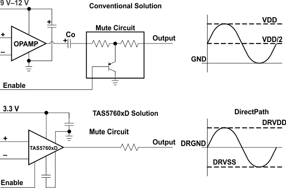
Single-supply line-driver amplifiers typically require dc-blocking capacitors. The top drawing in Figure 58 illustrates the conventional line-driver amplifier connection to the load and output signal. DC blocking capacitors are often large in value. The line load (typical resistive values of 600 Ω to 10 kΩ) combines with the dc blocking capacitors to form a high-pass filter. Equation 3 shows the relationship between the load impedance (RL), the capacitor (CO), and the cutoff frequency (fC).

CO can be determined using Equation 4, where the load impedance and the cutoff frequency are known.

If fC is low, the capacitor must then have a large value because the load resistance is small. Large capacitance values require large package sizes. Large package sizes consume PCB area, stand high above the PCB, increase cost of assembly, and can reduce the fidelity of the audio output signal.
The DirectPath amplifier architecture operates from a single supply but makes use of an internal charge pump to provide a negative voltage rail. Combining the user-provided positive rail and the negative rail generated by the IC, the device operates in what is effectively a split-supply mode. The output voltages are now centered at zero volts with the capability to swing to the positive rail or negative rail. Combining this with the built-in click and pop reduction circuit, the DirectPath amplifier requires no output dc blocking capacitors. The bottom block diagram and waveform of Figure 58 illustrate the ground-referenced line-driver architecture. This is the architecture of the headphone / line driver inside of the TAS5760LD.
