ZHCSDC1D September 2013 – October 2018 TAS5766M , TAS5768M
PRODUCTION DATA.
- 1 特性
- 2 应用
- 3 说明
- 4 修订历史记录
- 5 Pin Configuration and Functions
- 6 Specifications
-
7 Detailed Description
- 7.1 Overview
- 7.2 Functional Block Diagram
- 7.3 Feature Description
- 7.4
Device Functional Modes
- 7.4.1 Device Protection System
- 7.4.2 Reset and System Clock Functions
- 7.4.3 System Clock PLL Mode
- 7.4.4 Clock Generation and PLL
- 7.4.5 PLL Calculation
- 7.4.6 Audio Data Interface
- 7.4.7
TAS576xM Audio Processing Options
- 7.4.7.1 Overview
- 7.4.7.2 miniDSP Instruction Register
- 7.4.7.3 Digital Output
- 7.4.7.4 Software
- 7.4.7.5 Process Flow
- 7.4.7.6 Zero Data Detect
- 7.4.7.7 Power Save Modes
- 7.4.7.8 XSMT Pin (Soft Mute/Soft Un-Mute)
- 7.4.7.9 External Power Sense Undervoltage Protection Mode
- 7.4.7.10 Recommended Power Down Sequence
- 7.5 Programming
- 7.6 Register Maps
- 8 Applications and Implementation
- 9 Power Supply Recommendations
- 10Layout
-
11Register Map Information
- 11.1
Detailed Register Map Descriptions
- 11.1.1 Register Map Summary
- 11.1.2
Page 0 Registers
- 11.1.2.1 Page 0 / Register 1 (Hex 0x01)
- 11.1.2.2 Page 0 / Register 2 (Hex 0x02)
- 11.1.2.3 Page 0 / Register 3 (Hex 0x03)
- 11.1.2.4 Page 0 / Register 4 (Hex 0x04)
- 11.1.2.5 Page 0 / Register 7 (Hex 0x07)
- 11.1.2.6 Page 0 / Register 8 (Hex 0x08)
- 11.1.2.7 Page 0 / Register 9 (Hex 0x09)
- 11.1.2.8 Page 0 / Register 10 (Hex 0x0A)
- 11.1.2.9 Page 0 / Register 12 (Hex 0x0C)
- 11.1.2.10 Page 0 / Register 13 (Hex 0x0D)
- 11.1.2.11 Page 0 / Register 20 (Hex 0x14)
- 11.1.2.12 Page 0 / Register 21 (Hex 0x15)
- 11.1.2.13 Page 0 / Register 22 (Hex 0x16)
- 11.1.2.14 Page 0 / Register 23 (Hex 0x17)
- 11.1.2.15 Page 0 / Register 24 (Hex 0x18)
- 11.1.2.16 Page 0 / Register 27 (Hex 0x1B)
- 11.1.2.17 Page 0 / Register 28 (Hex 0x1C)
- 11.1.2.18 Page 0 / Register 29 (Hex 0x1D)
- 11.1.2.19 Page 0 / Register 30 (Hex 0x1E)
- 11.1.2.20 Page 0 / Register 32 (Hex 0x20)
- 11.1.2.21 Page 0 / Register 33 (Hex 0x21)
- 11.1.2.22 Page 0 / Register 34 (Hex 0x22)
- 11.1.2.23 Page 0 / Register 35 (Hex 0x23)
- 11.1.2.24 Page 0 / Register 36 (Hex 0x24)
- 11.1.2.25 Page 0 / Register 37 (Hex 0x25)
- 11.1.2.26 Page 0 / Register 40 (Hex 0x28)
- 11.1.2.27 Page 0 / Register 41 (Hex 0x29)
- 11.1.2.28 Page 0 / Register 42 (Hex 0x2A)
- 11.1.2.29 Page 0 / Register 43 (Hex 0x2B)
- 11.1.2.30 Page 0 / Register 44 (Hex 0x2C)
- 11.1.2.31 Page 0 / Register 59 (Hex 0x3B)
- 11.1.2.32 Page 0 / Register 65 (Hex 0x41)
- 11.1.2.33 Page 0 / Register 66 (Hex 0x42)
- 11.1.2.34 Page 0 / Register 82 (Hex 0x52)
- 11.1.2.35 Page 0 / Register 83 (Hex 0x53)
- 11.1.2.36 Page 0 / Register 84 (Hex 0x54)
- 11.1.2.37 Page 0 / Register 85 (Hex 0x55)
- 11.1.2.38 Page 0 / Register 86 (Hex 0x56)
- 11.1.2.39 Page 0 / Register 87 (Hex 0x57)
- 11.1.2.40 Page 0 / Register 90 (Hex 0x5A)
- 11.1.2.41 Page 0 / Register 91 (Hex 0x5B)
- 11.1.2.42 Page 0 / Register 92 (Hex 0x5C)
- 11.1.2.43 Page 0 / Register 93 (Hex 0x5D)
- 11.1.2.44 Page 0 / Register 94 (Hex 0x5E)
- 11.1.2.45 Page 0 / Register 95 (Hex 0x5F)
- 11.1.2.46 Page 0 / Register 108 (Hex 0x6C)
- 11.1.2.47 Page 0 / Register 118 (Hex 0x76)
- 11.1.2.48 Page 0 / Register 119 (Hex 0x77)
- 11.1.2.49 Page 0 / Register 120 (Hex 0x78)
- 11.1.2.50 Page 0 / Register 121 (Hex 0x79)
- 11.1.3 Page 1 Registers
- 11.1.4 Page 44 Registers
- 11.1
Detailed Register Map Descriptions
- 12器件和文档支持
- 13机械、封装和可订购信息
封装选项
机械数据 (封装 | 引脚)
散热焊盘机械数据 (封装 | 引脚)
- DCA|48
订购信息
7.4.7.9 External Power Sense Undervoltage Protection Mode
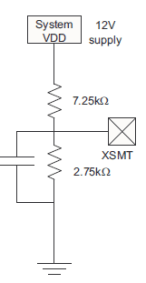
The XSMT pin can also be used to monitor a system voltage, such as the 24-VDC LCD TV back light, or 12-VDC system supply using a voltage divider created with two resistors. See Figure 45.
| * | If the XSMT pin makes a transition from “1” to “0” over 6ms or more, the device switches into external undervoltage protection mode. This mode uses two trigger levels. |  |
| * | When the XSMT pin level reaches 2 V, soft mute process begins. | |
| * | When the XSMT pin level reaches 1.2 V, analog mute engages, regardless of digital audio level, and analog shutdown begins. (DAC and related circuitry powers down). | |
| Figure 45. External Power Sense |
A timing diagram describing this is shown in Figure 46.
NOTE
The XSMT input pin voltage range is from –0.3 V to DVDD + 0.3 V.The ratio of external resistors must produce a voltage within this input range. Any increase in power supply (such as power supply positive noise or ripple) can pull the XSMT pin higher than DVDD +0.3V.
For example, if the TAS576xM is monitoring a 12 V input, and dividing the voltage by 4, then the voltage at XSMT during ideal power supply conditions is 3 V. A voltage spike higher than 14.4 V causes a voltage greater than 3.6 V (DVDD+0.3) on the XSMT pin, potentially damaging the device. Providing the divider is set appropriately, any DC voltage can be monitored.
 Figure 46. XSMT Timing for Undervoltage Protection