ZHCSI92D May 2018 – November 2020 TAS5805M
PRODUCTION DATA
- 1 特性
- 2 应用
- 3 说明
- 4 Revision History
- 5 Device Comparison Table
- 5 Pin Configuration and Functions
-
6 Specifications
- 6.1 Absolute Maximum Ratings
- 6.2 ESD Ratings
- 6.3 Recommended Operating Conditions
- 6.4 Thermal Information
- 6.5 Electrical Characteristics
- 6.6 Timing Requirements
- 6.7
Typical Characteristics
- 6.7.1 Bridge Tied Load (BTL) Configuration Curves with 1SPW Mode
- 6.7.2 Bridge Tied Load (BTL) Configuration Curves with BD Mode
- 6.7.3 Bridge Tied Load (BTL) Configuration Curves with Ferrite Bead + Capacitor as the Output Filter
- 6.7.4 Parallel Bridge Tied Load (PBTL) Configuration with 1SPW Modulation
- 6.7.5 Parallel Bridge Tied Load (PBTL) Configuration with BD Modulation
- 7 Parameter Measurement Information
-
7 Detailed Description
- 7.1 Overview
- 7.2 Functional Block Diagram
- 7.3 Feature Description
- 7.4 Device Functional Modes
- 7.5 Programming and Control
- 7.6 Register Maps
- 8 Application and Implementation
- 9 Power Supply Recommendations
- 9 Layout
- 10Device and Documentation Support
- 11Mechanical, Packaging, and Orderable Information
封装选项
请参考 PDF 数据表获取器件具体的封装图。
机械数据 (封装 | 引脚)
- PWP|28
散热焊盘机械数据 (封装 | 引脚)
- PWP|28
订购信息
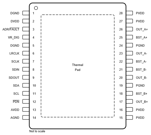
5 Pin Configuration and Functions
 Figure 5-1 PWP Package,28-Pin TSSOP,
Table 5-1 Pin Functions
| PIN | TYPE(1) | DESCRIPTION | |
|---|---|---|---|
| NAME | NO. | ||
| DGND | 1, 5 | P | Digital ground |
| DVDD | 2 | P | 3.3-V or 1.8-V digital power supply |
| VR_DIG | 4 | P | Internally regulated 1.5-V digital supply voltage. This pin must not be used to drive external devices |
| ADR/ FAULT | 3 | DI/O | Different I2 C device address can be set by selecting different pull up resistor to DVDD, see Table 7-5 for details. After power up, ADR/ FAULT can be redefine as FAULT, go to Page0, Book0, set register 0x61 = 0x0b first, then set register 0x60 = 0x01 |
| LRCLK | 6 | DI | Word select clock for the digital signal that is active on the serial port's input data line. In I2S, LJ and RJ, this corresponds to the left channel and right channel boundary. In TDM mode, this corresponds to the frame sync boundary |
| SCLK | 7 | DI | Bit clock for the digital signal that is active on the input data line of the serial data port. |
| SDIN | 8 | DI | Data line to the serial data port |
| SDOUT | 9 | DO | Serial Audio data output. The source data can be Pre-DSP or Post-DSP data, by setting the register 0x30h. |
| SDA | 10 | DI/O | I2C serial control data interface input/output |
| SCL | 11 | DI | I2C serial control clock input |
| PDN | 12 | DI | Power Down, active-low. PDN place the amplifier in Shutdown, turn off all internal regulators. Low, Power Down Device; High, Enable Device. |
| AVDD | 13 | P | Internally regulated 5-V analog supply voltage. This pin must not be used to drive external devices |
| AGND | 14 | P | Analog ground |
| PVDD | 15,16,27,28 | P | PVDD voltage input |
| PGND | 19,24 | P | Ground reference for power device circuitry. Connect this pin to system ground. |
| OUT_A+ | 26 | O | Positive pin for differential speaker amplifier output A+ |
| BST_A+ | 25 | P | Connection point for the OUT_A+ bootstrap capacitor which is used to create a power supply for the high-side gate drive for OUT_A+ |
| OUT_A- | 23 | O | Negative pin for differential speaker amplifier output A- |
| BST_A- | 22 | P | Connection point for the OUT_A- bootstrap capacitor which is used to create a power supply for the high-side gate drive for OUT_A- |
| BST_B- | 21 | P | Connection point for the OUT_B- bootstrap capacitor which is used to create a power supply for the high-side gate drive for OUT_B- |
| OUT_B- | 20 | O | Negative pin for differential speaker amplifier output B |
| BST_B+ | 18 | P | Connection point for the OUT_B+ bootstrap capacitor which is used to create a power supply for the high-side gate drive for OUT_B+ |
| OUT_B+ | 17 | O | Positive pin for differential speaker amplifier output B+ |
| PowerPAD™ | P | Connect to the system Ground | |
(1) AI = Analog input, AO = Analog output, DI = Digital Input, DO =
Digital Output, DI/O = Digital Bi-directional (input and output), P = Power, G =
Ground (0 V)