ZHCSMV1
December 2020
TAS5822M
PRODUCTION DATA
1
特性
2
应用
3
说明
4
Revision History
5
Pin Configuration and Functions
6
Specifications
6.1
Absolute Maximum Ratings
6.2
ESD Ratings
6.3
Recommended Operating Conditions
6.4
Thermal Information
6.5
Electrical Characteristics
6.6
Timing Requirements
6.7
Typical Characteristics
6.7.1
Bridge Tied Load (BTL) Configuration Curves with 1SPW Modulation, Fsw = 768kHz
6.7.2
Parallel Bridge Tied Load (PBTL) Configuration Curves with 1SPW Modulation, Fsw = 768kHz
6.8
Parametric Measurement Information
6.8.1
Power Consumption Summary
7
Detailed Description
7.1
Overview
7.2
Functional Block Diagram
7.3
Feature Description
7.3.1
Power Supplies
7.3.2
Device Clocking
7.3.3
Serial Audio Port – Clock Rates
7.3.4
Clock Halt Auto-recovery
7.3.5
Sample Rate on the Fly Change
7.3.6
Serial Audio Port - Data Formats and Bit Depths
7.3.7
Digital Audio Processing
7.3.8
Class D Audio Amplifier
7.3.8.1
Speaker Amplifier Gain Select
7.4
Device Functional Modes
7.4.1
Software Control
7.4.2
Speaker Amplifier Operating Modes
7.4.2.1
BTL Mode
7.4.2.2
PBTL Mode
7.4.3
Minimize EMI with Spread Spectrum
7.4.4
Minimize EMI with channel to channel phase shift
7.4.5
Minimize EMI with Multi-Devices PWM Phase Synchronization
7.4.6
Thermal Foldback
7.4.7
Device State Control
7.4.8
Device Modulation
7.4.8.1
BD Modulation
7.4.8.2
1SPW Modulation
7.4.8.3
Hybrid Modulation
7.5
Programming and Control
7.5.1
I2 C Serial Communication Bus
7.5.2
Slave Address
7.5.2.1
Random Write
7.5.2.2
Sequential Write
7.5.2.3
Random Read
7.5.2.4
Sequential Read
7.5.2.5
DSP Memory Book, Page and BQ update
7.5.2.6
Example Use
7.5.2.7
Checksum
7.5.2.7.1
Cyclic Redundancy Check (CRC) Checksum
7.5.2.7.2
Exclusive or (XOR) Checksum
7.5.3
Control via Software
7.5.3.1
Startup Procedures
7.5.3.2
Shutdown Procedures
7.5.3.3
Protection and Monitoring
7.5.3.3.1
Over current Shutdown (OCSD)
7.5.3.3.2
Speaker DC Protection
7.5.3.3.3
Device Over Temperature Protection
7.5.3.3.4
Over Voltage Protection
7.5.3.3.5
Under Voltage Protection
7.5.3.3.6
Clock Fault
7.6
Register Maps
7.6.1
CONTROL PORT Registers
8
Application and Implementation
8.1
Application Information
8.2
Typical Applications
8.2.1
2.0 (Stereo BTL) System
8.2.2
MONO (PBTL) System
8.2.2.1
Design Requirements
8.2.2.2
Detailed Design Procedure
8.2.2.2.1
Bootstrap Capacitors
8.2.2.2.2
Inductor Selections
8.2.2.2.3
Power Supply Decoupling
8.2.2.2.4
Output EMI Filtering
8.2.2.3
Application Performance Plots
9
Power Supply Recommendations
9.1
DVDD Supply
9.2
PVDD Supply
10
Layout
10.1
Layout Guidelines
10.1.1
General Guidelines for Audio Amplifiers
10.1.2
Importance of PVDD Bypass Capacitor Placement on PVDD Network
10.1.3
Optimizing Thermal Performance
10.1.3.1
Device, Copper, and Component Layout
10.1.3.2
Stencil Pattern
10.1.3.2.1
PCB footprint and Via Arrangement
10.1.3.2.2
Solder Stencil
10.2
Layout Example
11
Device and Documentation Support
11.1
支持资源
11.2
Trademarks
11.3
静电放电警告
11.4
术语表
12
Mechanical, Packaging, and Orderable Information
封装选项
机械数据 (封装 | 引脚)
DCP|38
MPDS520B
散热焊盘机械数据 (封装 | 引脚)
DCP|38
PPTD170A
订购信息
zhcsmv1_oa
zhcsmv1_pm
8.2.2.3
Application Performance Plots
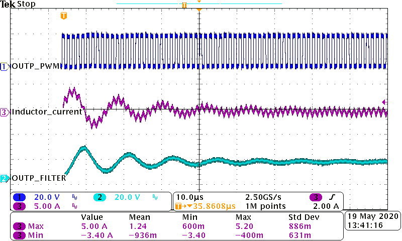
Figure 8-3
Start-up Current
(Fsw = 768 kHz, LC filter = 4.7 µH + 0.68 µF, PVDD = 24 V, BD Modulation)
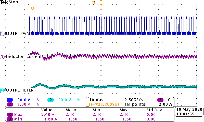
Figure 8-4
Start-up Current
(Fsw = 768 kHz, LC filter = 4.7 µH + 0.68 µF, PVDD = 24 V, 1SPW Modulation)
千亿体育app官网登录(中国)官方网站IOS/安卓通用版/手机APP
|
米乐app下载官网(中国)|ios|Android/通用版APP最新版
|
米乐|米乐·M6(中国大陆)官方网站
|
千亿体育登陆地址
|
华体会体育(中国)HTH·官方网站
|
千赢qy国际_全站最新版千赢qy国际V6.2.14安卓/IOS下载
|
18新利网v1.2.5|中国官方网站
|
bob电竞真人(中国官网)安卓/ios苹果/电脑版【1.97.95版下载】
|
千亿体育app官方下载(中国)官方网站IOS/安卓/手机APP下载安装
|