ZHCSO77A June   2021  – December 2021 TAS5828M

PRODUCTION DATA  

  1. 特性
  2. 应用
  3. 说明
  4. Revision History
  5. Pin Configuration and Functions
  6. Specifications
    1. 6.1 Absolute Maximum Ratings
    2. 6.2 ESD Ratings
    3. 6.3 Recommended Operating Conditions
    4. 6.4 Thermal Information
    5. 6.5 Electrical Characteristics
    6. 6.6 Timing Requirements
    7. 6.7 Typical Characteristics
      1. 6.7.1 Bridge Tied Load (BTL) Configuration Curves with BD Modulation
      2. 6.7.2 Bridge Tied Load (BTL) Configuration Curves with 1SPW Modulation
      3. 6.7.3 Parallel Bridge Tied Load (PBTL) Configuration With BD Modulation
      4. 6.7.4 Parallel Bridge Tied Load (PBTL) Configuration With 1SPW Modulation
  7. Parameter Measurement Information
  8. Detailed Description
    1. 8.1 Overview
    2. 8.2 Functional Block Diagram
    3. 8.3 Feature Description
      1. 8.3.1 Power Supplies
      2. 8.3.2 Device Clocking
      3. 8.3.3 Serial Audio Port – Clock Rates
      4. 8.3.4 Clock Halt Auto-recovery
      5. 8.3.5 Sample Rate on the Fly Change
      6. 8.3.6 Serial Audio Port - Data Formats and Bit Depths
      7. 8.3.7 Digital Audio Processing
      8. 8.3.8 Class D Audio Amplifier
        1. 8.3.8.1 Speaker Amplifier Gain Select
        2. 8.3.8.2 Class D Loop Bandwidth and Switching Frequency Setting
    4. 8.4 Device Functional Modes
      1. 8.4.1 Software Control
      2. 8.4.2 Speaker Amplifier Operating Modes
        1. 8.4.2.1 BTL Mode
        2. 8.4.2.2 PBTL Mode
      3. 8.4.3 Low EMI Modes
        1. 8.4.3.1 Spread Spectrum
        2. 8.4.3.2 Channel to Channel Phase Shift
        3. 8.4.3.3 Multi-Devices PWM Phase Synchronization
          1. 8.4.3.3.1 Phase Synchronization With I2S Clock In Startup Phase
          2. 8.4.3.3.2 Phase Synchronization With GPIO
      4. 8.4.4 Thermal Foldback
      5. 8.4.5 Device State Control
      6. 8.4.6 Device Modulation
        1. 8.4.6.1 BD Modulation
        2. 8.4.6.2 1SPW Modulation
        3. 8.4.6.3 Hybrid Modulation
    5. 8.5 Programming and Control
      1. 8.5.1 I2 C Serial Communication Bus
      2. 8.5.2 Hardware Control Mode
      3. 8.5.3 I2 C Target Address
        1. 8.5.3.1 Random Write
        2. 8.5.3.2 Sequential Write
        3. 8.5.3.3 Random Read
        4. 8.5.3.4 Sequential Read
        5. 8.5.3.5 DSP Memory Book, Page and BQ update
        6. 8.5.3.6 Checksum
          1. 8.5.3.6.1 Cyclic Redundancy Check (CRC) Checksum
          2. 8.5.3.6.2 Exclusive or (XOR) Checksum
      4. 8.5.4 Control via Software
        1. 8.5.4.1 Startup Procedures
        2. 8.5.4.2 Shutdown Procedures
      5. 8.5.5 Protection and Monitoring
        1. 8.5.5.1 Overcurrent Limit (Cycle-By-Cycle)
        2. 8.5.5.2 Overcurrent Shutdown (OCSD)
        3. 8.5.5.3 DC Detect Error
        4. 8.5.5.4 Overtemperature Shutdown (OTSD)
        5. 8.5.5.5 PVDD Overvoltage and Undervoltage Error
        6. 8.5.5.6 PVDD Drop Detection
        7. 8.5.5.7 Clock Fault
    6. 8.6 Register Maps
      1. 8.6.1 CONTROL PORT Registers
  9. Application and Implementation
    1. 9.1 Application Information
      1. 9.1.1 Inductor Selections
      2. 9.1.2 Bootstrap Capacitors
      3. 9.1.3 Power Supply Decoupling
      4. 9.1.4 Output EMI Filtering
    2. 9.2 Typical Applications
      1. 9.2.1 2.0 (Stereo BTL) System
      2. 9.2.2 Design Requirements
      3. 9.2.3 Detailed Design procedures
        1. 9.2.3.1 Step One: Hardware Integration
        2. 9.2.3.2 Step Two: Hardware Integration
        3. 9.2.3.3 Step Three: Software Integration
      4. 9.2.4 MONO (PBTL) Systems
      5. 9.2.5 Advanced 2.1 System (Two TAS5828M Devices)
  10. 10Power Supply Recommendations
    1. 10.1 DVDD Supply
    2. 10.2 PVDD Supply
  11. 11Layout
    1. 11.1 Layout Guidelines
      1. 11.1.1 General Guidelines for Audio Amplifiers
      2. 11.1.2 Importance of PVDD Bypass Capacitor Placement on PVDD Network
      3. 11.1.3 Optimizing Thermal Performance
        1. 11.1.3.1 Device, Copper, and Component Layout
        2. 11.1.3.2 Stencil Pattern
          1. 11.1.3.2.1 PCB footprint and Via Arrangement
          2. 11.1.3.2.2 Solder Stencil
    2. 11.2 Layout Example
  12. 12Device and Documentation Support
    1. 12.1 Device Support
      1. 12.1.1 Device Nomenclature
      2. 12.1.2 Development Support
    2. 12.2 Receiving Notification of Documentation Updates
    3. 12.3 Support Resources
    4. 12.4 Trademarks
    5. 12.5 Electrostatic Discharge Caution
    6. 12.6 Glossary
  13. 13Mechanical, Packaging, and Orderable Information

封装选项

请参考 PDF 数据表获取器件具体的封装图。

机械数据 (封装 | 引脚)
  • DAD|32
散热焊盘机械数据 (封装 | 引脚)
订购信息

Speaker Amplifier Gain Select

A combination of digital gain and analog gain is used to provide the overall gain of the speaker amplifier. As seen in Figure 8-7, the audio path of the TAS5828M consists of a digital audio input port, a digital audio path, a digital to PWM converter (DPC), a gate driver stage, a Class D power stage, and a feedback loop which feeds the output information back into the DPC block to correct for distortion sensed on the output pins. The total amplifier gain is comprised of digital gain, shown in the digital audio path and the analog gain from the input of the analog modulator to the output of the speaker amplifier power stage.
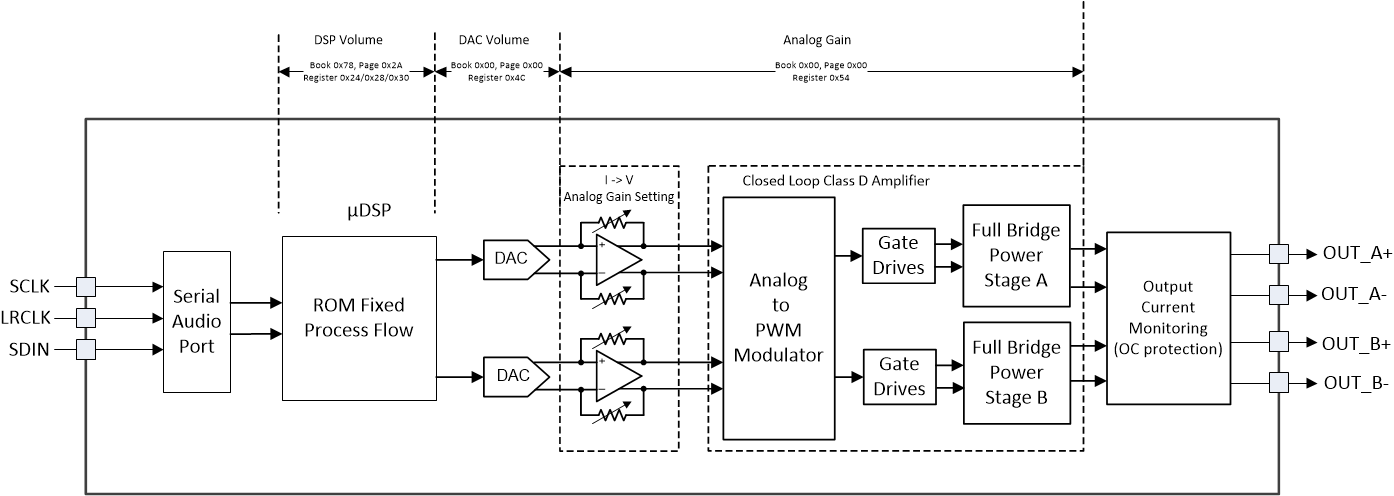
GUID-6404F001-3AE4-47EC-B195-D6065CD8CA5C-low.gif Figure 8-7 Speaker Amplifier Gain

As shown in Figure 8-7, the first gain stage for the speaker amplifier is present in the digital audio path. It consists of the volume control and the digital boost block. The volume control is set to 0 dB by default, it does not change. For all settings of the register 0x54, AGAIN[4:0], the digital boost block remains at 0 dB. These gain settings ensure that the output signal is not clipping at different PVDD levels. 0dBFS output is 29.5-V peak output voltage

Table 8-2 Analog Gain Setting
AGAIN <4:0> GAIN (dBFS) AMPLIFIER OUTPUT PEAK VOLTAGE (VP/FS) AMPLIFIER OUTPUT PEAK VOLTAGE (dBVP/FS)
00000 0 29.5 29.4
00001 -0.5 27.85 28.9
00010 -1.0 26.29 28.4
00011 -1.5 24.82 27.9
……. …….. ……. …….
11111 -15.5 4.95 13.9