ZHCSFZ6 December 2016 TAS6422-Q1
PRODUCTION DATA.
- 1 特性
- 2 应用
- 3 说明
- 4 修订历史记录
- 5 说明(续)
- 6 Device Comparison Table
- 7 Pin Configuration and Functions
- 8 Specifications
- 9 Parameter measurement Information
-
10Detailed description
- 10.1 Overview
- 10.2 Functional Block Diagram
- 10.3
Feature Description
- 10.3.1 Serial Audio Port
- 10.3.2 High-Pass Filter
- 10.3.3 Volume Control and Gain
- 10.3.4 High-Frequency Pulse-Width Modulator (PWM)
- 10.3.5 Gate Drive
- 10.3.6 Power FETs
- 10.3.7 Load Diagnostics
- 10.3.8
Protection and Monitoring
- 10.3.8.1 Overcurrent Limit (ILIMIT)
- 10.3.8.2 Overcurrent Shutdown (ISD)
- 10.3.8.3 DC Detect
- 10.3.8.4 Clip Detect
- 10.3.8.5 Global Overtemperature Warning (OTW), Overtemperature Shutdown (OTSD)
- 10.3.8.6 Channel Overtemperature Warning [OTW(i)] and Shutdown [OTSD(i)]
- 10.3.8.7 Undervoltage (UV) and Power-On-Reset (POR)
- 10.3.8.8 Overvoltage (OV) and Load Dump
- 10.3.9 Power Supply
- 10.3.10 Hardware Control Pins
- 10.4 Device Functional Modes
- 10.5 Programming
- 10.6
Register Maps
- 10.6.1 Mode Control Register (address = 0x00) [default = 0x00]
- 10.6.2 Miscellaneous Control 1 Register (address = 0x01) [default = 0x32]
- 10.6.3 Miscellaneous Control 2 Register (address = 0x02) [default = 0x62]
- 10.6.4 SAP Control (Serial Audio-Port Control) Register (address = 0x03) [default = 0x04]
- 10.6.5 Channel State Control Register (address = 0x04) [default = 0x55]
- 10.6.6 Channel 1 Through 2 Volume Control Registers (address = 0x05-0x06) [default = 0xCF]
- 10.6.7 DC Load Diagnostic Control 1 Register (address = 0x09) [default = 0x00]
- 10.6.8 DC Load Diagnostic Control 2 Register (address = 0x0A) [default = 0x11]
- 10.6.9 DC Load Diagnostic Report 1 Register (address = 0x0C) [default = 0x00]
- 10.6.10 DC Load Diagnostics Report 3 Line Output Register (address = 0x0E) [default = 0x00]
- 10.6.11 Channel State Reporting Register (address = 0x0F) [default = 0x55]
- 10.6.12 Channel Faults (Overcurrent, DC Detection) Register (address = 0x10) [default = 0x00]
- 10.6.13 Global Faults 1 Register (address = 0x11) [default = 0x00]
- 10.6.14 Global Faults 2 Register (address = 0x12) [default = 0x00]
- 10.6.15 Warnings Register (address = 0x13) [default = 0x20]
- 10.6.16 Pin Control Register (address = 0x14) [default = 0x00]
- 10.6.17 AC Load Diagnostic Control 1 Register (address = 0x15) [default = 0x00]
- 10.6.18 AC Load Diagnostic Control 2 Register (address = 0x16) [default = 0x00]
- 10.6.19 AC Load Diagnostic Impedance Report Ch1 through CH2 Registers (address = 0x17-0x18) [default = 0x00]
- 10.6.20 AC Load Diagnostic Phase Report High Register (address = 0x1B) [default = 0x00]
- 10.6.21 AC Load Diagnostic Phase Report Low Register (address = 0x1C) [default = 0x00]
- 10.6.22 AC Load Diagnostic STI Report High Register (address = 0x1D) [default = 0x00]
- 10.6.23 AC Load Diagnostic STI Report Low Register (address = 0x1E) [default = 0x00]
- 10.6.24 Miscellaneous Control 3 Register (address = 0x21) [default = 0x00]
- 10.6.25 Clip Control Register (address = 0x22) [default = 0x01]
- 10.6.26 Clip Window Register (address = 0x23) [default = 0x14]
- 10.6.27 Clip Warning Register (address = 0x24) [default = 0x00]
- 10.6.28 ILIMIT Status Register (address = 0x25) [default = 0x00]
- 10.6.29 Miscellaneous Control 4 Register (address = 0x26) [default = 0x40]
- 11Application and Implementation
- 12Power Supply Recommendations
- 13Layout
- 14器件和文档支持
- 15机械、封装和可订购信息
11 Application and Implementation
NOTE
Information in the following applications sections is not part of the TI component specification, and TI does not warrant its accuracy or completeness. TI’s customers are responsible for determining suitability of components for their purposes. Customers should validate and test their design implementation to confirm system functionality.
11.1 Application Information
The TAS6422-Q1 is a two-channel class-D digital-input audio-amplifier design for use in automotive head units and external amplifier modules. The TAS6422-Q1 incorporates the necessary functionality to perform in demanding OEM applications.
11.1.1 AM-Radio Band Avoidance
AM-radio frequency interference can be avoided by setting the switching frequency of the device above the AM band. The switching frequency options available are 38 fs, 44 fs, and 48 fs. If the switch frequency cannot be set above the AM band, then use the two options of 8 fs and 10 fs. These options should be changed to avoid AM active channels.
11.1.2 Parallel BTL Operation (PBTL)
The device can drive more current-paralleling BTL channels on the load side of the LC output filter. For parallel operation, the parallel BTL mode, PBTL, must be used and the paralleled channels must have the same state in the state control register. If the two states are not aligned the device reports a fault condition.
To set the requested channels to PBTL mode the device must be in standby mode for the commands to take effect.
A load diagnostic is supported for PBTL channels. Paralleling on the device side of the LC output filter is not supported.
11.1.3 Demodulation Filter Design
The amplifier outputs are driven by high-current LDMOS transistors in an H-bridge configuration. These transistors are either fully off or fully on. The result is a square-wave output signal with a duty cycle that is proportional to the amplitude of the audio signal. An LC demodulation filter is used to recover the audio signal. The filter attenuates the high-frequency components of the output signals that are out of the audio band. The design of the demodulation filter significantly affects the audio performance of the power amplifier. Therefore, to meet the system THD+N requirements, the selection of the inductors used in the output filter should be carefully considered.
11.1.4 Line Driver Applications
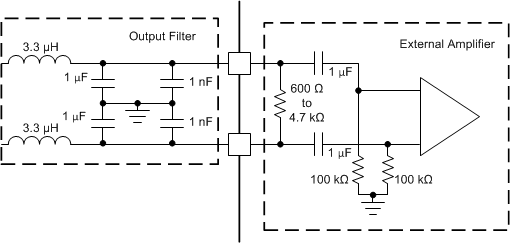
In many automotive audio applications, the same head unit must drive either a speaker (with several ohms of impedance) or an external amplifier input (with several kiloohms of impedance). The design is capable of supporting both applications and has special line-drive gain and diagnostics. Coupled with the high switching frequency, the device is well suited for this type of application. Set the desired channel in line driver mode through I2C register 0x00, the externally connected amplifier must have a differential impedance from 600 Ω to 4.7 kΩ for the DC line diagnostic to detect the connected external amplifier. Figure 75 shows the recommended external amplifier input configuration.
 Figure 75. External Amplifier Input Configuration for Line Driver
11.2 Typical Application
11.2.1 BTL Application
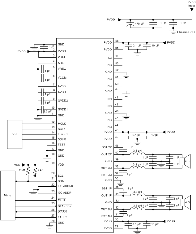
Figure 76 shows the schematic of a typical 2-channel solution for a head-rest amplifier application.
 Figure 76. TAS6422-Q1 Typical 2-Channel BTL Application Schematic
11.2.1.1 Design Requirements
Use the following requirements for this design:
- This headrest amplifier example is focused on the smallest solution size for 2 × 50 W output power into 2 Ω with a battery supply of 14.4 V.
- The switching frequency is set above the AM-band with 44 times the input sample rate of 48 kHz which results in a frequency of 2.11 MHz.
- The selection of a 2.11 MHz switch frequency enables the use of a small output inductor value of 3.3 µH which leads to a very small solution size.
11.2.1.2 Communication
All communications to the TAS6422-Q1 are through the I2C protocol. A system controller can communicate with the device through the SDA pins and SCL pins. The TAS6422-Q1 is an I2C slave device and requires a master. The device cannot generate an I2C clock or initiate a transaction. The maximum clock speed accepted by the device is 400 kHz. If multiple TAS6422-Q1 devices are on the same I2C bus, the I2C address must be different for each device. Up to four TAS6422-Q1 devices can be on the same I2C bus.
The I2C bus is shared internally.
NOTE
Complete any internal operations, such as load diagnostics, before reading the registers for the results.
11.2.1.3 Detailed Design Procedure
11.2.1.3.1 Hardware Design
Use the following procedure for the hardware design:
- Determine the input format. The input format can be either I2S or TDM mode. The mode determines the correct pin connections and the I2C register settings.
- Determine the power output that is required into the load. The power requirement determines the required power-supply voltage and current. The output reconstruction-filter components that are required are also driven by the output power.
- With the requirements, adjust the typical application schematic in Figure 76 for the input connections.
11.2.1.3.2 Digital Input and the Serial Audio Port
The TAS6422-Q1 device supports four different digital input formats which are: I2S, Right Justified, Left Justified, and TDM mode. Depending on the format, the device can support 16, 18, 20, 24, and 32 bit data. The supported frequencies are 96 kHz, 48 kHz, and 44.1 kHz. Please see Table 13 for the I2C register, SAP Control, for the complete matrix to set up the serial audio port.
NOTE
Bits 3, 4, and 5 in this register are ignored in all input formats except for TDM. Setting up all the control registers to the system requirements should be done before the device is placed in Mute mode or Play mode. After the registers are setup, use bit 7 in register 0x21 to clear any faults. Then read the fault registers to make sure no faults are present. When no faults are present, use register 0x04 to place the device properly into play mode.
11.2.1.3.3 Bootstrap Capacitors
The bootstrap capacitors provide the gate-drive voltage of the upper N-channel FET. These capacitors must be sized appropriately for the system specification. A special condition can occur where the bootstrap may sag if the capacitor is not sized accordingly. The special condition is just below clipping where the PWM is slightly less than 100% duty cycle with sustained low-frequency signals. Changing the bootstrap capacitor value to 2.2 µF for driving subwoofers that require frequencies below 30 Hz may be necessary.
11.2.1.3.4 Output Reconstruction Filter
The output FETs drive the amplifier outputs in an H-Bridge configuration. These transistors are either fully off or fully on. The result is a square-wave output signal with a duty cycle that is proportional to the amplitude of the audio signal. The amplifier outputs require a reconstruction filter that comprises a series inductor and a capacitor to ground on each output, generally called an LC filter. The LC filter attenuates the PWM frequency and reduces electromagnetic emissions, allowing the reconstructed audio signal to pass to the speakers. refer to the Class-D LC Filter Design, (SLOA119) for a detailed description of proper component description and design of the LC filter based upon the specified load and frequency response. The recommended low-pass cutoff frequency of the LC filter is dependent on the selected switching frequency. The low-pass cutoff frequency can be as high as 100 kHz for a PWM frequency of 2.1 MHz. At a PWM frequency of 384 kHz the low-pass cutoff frequency should be less than 40 kHz. Certain specifications must be understood for a proper inductor. The inductance value is given at zero current, but the TAS6422-Q1 device will have current. Use the inductance versus current curve for the inductor to make sure the inductance does not drop below 1 µH (for fSW = 2.1 MHz) at the maximum current provided by the system design. The DCR of the inductor directly affects the output power of the system design. The lower the DCR, the more power is provided to the speakers. The typical inductor DCR for a 4 Ω system is 40 to 50 mΩ and for a 2 Ω system is 20 to 25 mΩ.
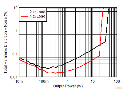
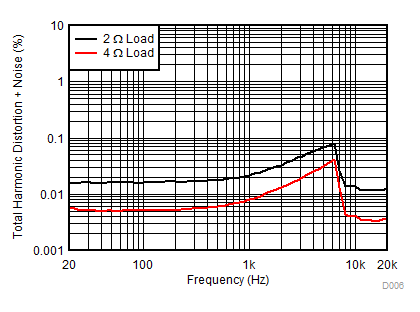
11.2.1.4 Application Curves

| 1 kHz | PVDD = 14.4 V |

| 1 W | PVDD = 14.4 V |