ZHCSPC7B December 2022 – November 2023 TCA39416
PRODUCTION DATA
7.3.1 Architecture
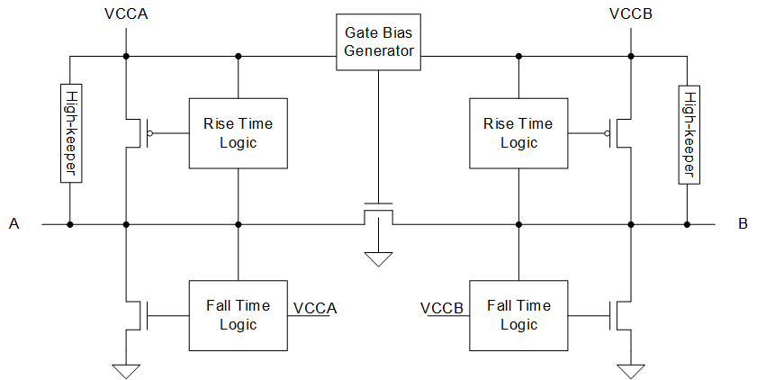
The TCA39416 architecture (see Figure 7-1) is an auto-direction-sensing based translator that does not require a direction-control signal to control the direction of data flow from A to B or from B to A.
 Figure 7-1 Architecture of a TCA39416 Cell
These two bidirectional channels support both directions of data flow without a direction-control signal. By properly biasing the gate of the pass-FET, the FET can turn on (low RDSON), when either side input voltage drops to ~ 1 voltage threshold below the lowest of the two supplies.
The TCA39416 is part of the TI "Switch" type voltage translator family and employs key circuits to enable this voltage translation:
- An N-channel pass-gate transistor topology that ties the A-port to the B-port.
- Output rise time accelerator circuitry to detect and accelerate rising edges on the A or B ports
- Output fall time accelerator circuitry to detect and accelerate falling edges on the A or B ports
For bidirectional voltage translation, pull up resistors are included on the device for dc current sourcing capability. The VGATE gate bias of the N-channel pass transistor is set to the lower supply voltage and can be represented with VCCA.
The rise and fall time accelerator (RTA and FTA, respectively) circuitry speeds up the output slew rate by monitoring the input edge for transitions, helping maintain the data rate through the device. During a low-to-high signal rising edge, the rise time accelerator (RTA) circuit turns on to increase the current drive capability of the driver. This edge-rate acceleration provides high ac drive by bypassing the internal 10-kΩ pull up resistors during the low-to-high transition to speed up the signal. The output resistance of the driver is decreased to approximately 150 Ω during this acceleration phase. During a high-to-low signal falling edge, the fall time accelerator (FTA) turns on to increase the current drive capability of the driver, similar to the rise time accelerator. This helps reduce the fall time for large capacitive loads. For light capacitive loads, the fall time accelerator will not enable.