ZHCS034C January   2011  – August 2018 TCA4311A

PRODUCTION DATA.  

  1. 特性
  2. 应用
  3. 说明
    1.     Device Images
      1.      简化原理图
  4. 修订历史记录
  5. Pin Configuration and Functions
    1.     Pin Functions
  6. Specifications
    1. 6.1 Absolute Maximum Ratings
    2. 6.2 ESD Ratings
    3. 6.3 Recommended Operating Conditions
    4. 6.4 Thermal Information
    5. 6.5 Electrical Characteristics
    6. 6.6 Typical Characteristics
  7. Parameter Measurement Information
  8. Detailed Description
    1. 8.1 Overview
    2. 8.2 Functional Block Diagram
    3. 8.3 Feature Description
      1. 8.3.1 Rise-Time Accelerators
      2. 8.3.2 READY Digital Output
      3. 8.3.3 EN Low Current Disable
    4. 8.4 Device Functional Modes
      1. 8.4.1 Start-Up
      2. 8.4.2 Connection Circuitry
      3. 8.4.3 Missing ACK Event
        1. 8.4.3.1 System Impact
        2. 8.4.3.2 System Workaround
  9. Application and Implementation
    1. 9.1 Application Information
    2. 9.2 Typical Application
      1. 9.2.1 Design Requirements
        1. 9.2.1.1 Input to Output Offset Voltage
        2. 9.2.1.2 Propagation Delays
      2. 9.2.2 Detailed Design Procedure
        1. 9.2.2.1 Resistor Pull-Up Value Selection
      3. 9.2.3 Application Curves
      4. 9.2.4 Live Insertion and Capacitance Buffering CompactPCI Application
        1. 9.2.4.1 Design Requirements
        2. 9.2.4.2 Detailed Design Procedure
        3. 9.2.4.3 Application Curves
      5. 9.2.5 Live Insertion and Capacitance Buffering PCI Application
        1. 9.2.5.1 Design Requirements
        2. 9.2.5.2 Detailed Design Procedure
        3. 9.2.5.3 Application Curves
      6. 9.2.6 Repeater/Bus Extender Application
        1. 9.2.6.1 Design Requirements
        2. 9.2.6.2 Detailed Design Procedure
        3. 9.2.6.3 Application Curves
      7. 9.2.7 Systems With Disparate Supply Voltages
        1. 9.2.7.1 Design Requirements
        2. 9.2.7.2 Detailed Design Procedure
        3. 9.2.7.3 Application Curves
  10. 10Power Supply Recommendations
  11. 11Layout
    1. 11.1 Layout Guidelines
    2. 11.2 Layout Example
  12. 12器件和文档支持
    1. 12.1 接收文档更新通知
    2. 12.2 社区资源
    3. 12.3 商标
    4. 12.4 静电放电警告
    5. 12.5 术语表
  13. 13机械、封装和可订购信息

封装选项

机械数据 (封装 | 引脚)
散热焊盘机械数据 (封装 | 引脚)
订购信息

Missing ACK Event

Description

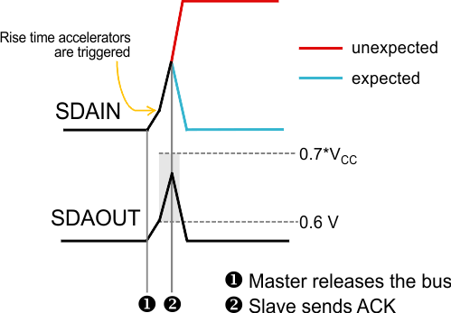
When the slave (or master) device sends an ACK bit, a logic low on SDA during the 9th clock cycle, the slave (or master) may pull the SDA line low while the rise time accelerators are engaged and the master (or slave) side stays high. The rise time accelerators are engaged when the voltage is above 0.6 V (typical) and the slew rate is above 1.25 V/us. In Figure 8, SDAOUT is a slave attempting to send an ACK bit. SDAOUT pulls to a logic low, but the ACK is not transferred to the other side and SDAIN remains high unexpectedly. The timing window in which this occurs has been approximated to 1 nanosecond and can vary with the loading on the bus.
TCA4311A errata_scps173.gifFigure 8. Missing ACK