ZHCS034C January 2011 – August 2018 TCA4311A
PRODUCTION DATA.
- 1 特性
- 2 应用
- 3 说明
- 4 修订历史记录
- 5 Pin Configuration and Functions
- 6 Specifications
- 7 Parameter Measurement Information
- 8 Detailed Description
-
9 Application and Implementation
- 9.1 Application Information
- 9.2
Typical Application
- 9.2.1 Design Requirements
- 9.2.2 Detailed Design Procedure
- 9.2.3 Application Curves
- 9.2.4 Live Insertion and Capacitance Buffering CompactPCI Application
- 9.2.5 Live Insertion and Capacitance Buffering PCI Application
- 9.2.6 Repeater/Bus Extender Application
- 9.2.7 Systems With Disparate Supply Voltages
- 10Power Supply Recommendations
- 11Layout
- 12器件和文档支持
- 13机械、封装和可订购信息
9.2.4 Live Insertion and Capacitance Buffering CompactPCI™ Application
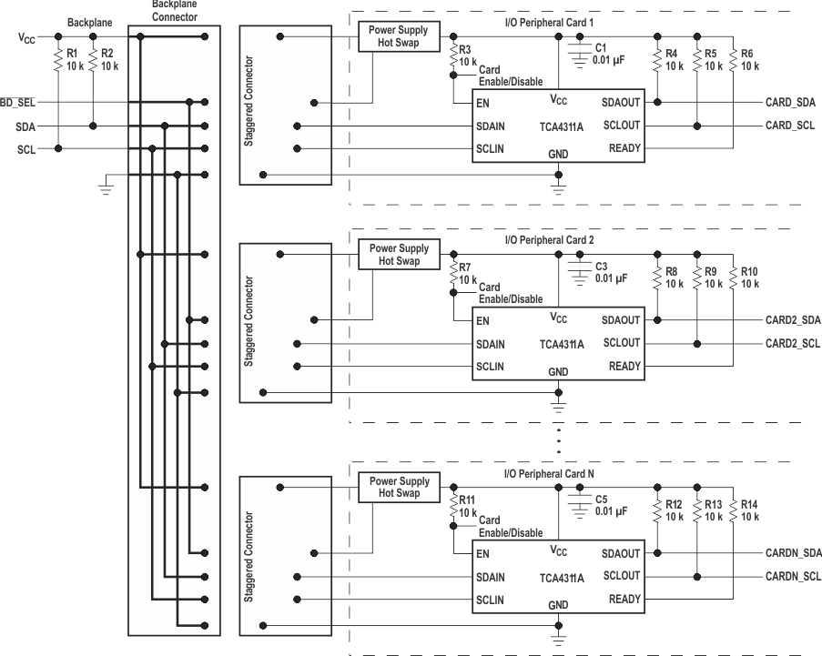
Figure 12 through Figure 13 illustrate the usage of the TCA4311A in applications that take advantage of both its hot swap controlling and capacitance buffering features. In all of these applications, note that if the I/O cards were plugged directly into the backplane, all of the backplane and card capacitances would add directly together, making rise- and fall-time requirements difficult to meet. Placing a TCA4311A on the edge of each card, however, isolates the card capacitance from the backplane. For a given I/O card, the TCA4311A drives the capacitance of everything on the card and the backplane must drive only the capacitance of the TCA4311A, which is less than 10 pF.
Figure 12 shows the TCA4311A in a CompactPCI™ configuration. Connect VCC and EN to the output of one of the CompactPCI™ power supply Hot Swap circuits. Use a pull-up resistor to EN for a card side enable/disable.
VCC is monitored by a filtered UVLO circuit. With the VCC voltage powering up after all other pins have established connection, the UVLO circuit ensures that the backplane and card data and clock busses are not connected until the transients associated with live insertion have settled. Owing to their small capacitance, the SDAIN and SCLIN pins cause minimal disturbance on the backplane busses when they make contact with the connector.
 Figure 12. Inserting Multiple I/O Cards into a Live Backplane Using the TCA4311A in a CompactPCI System