ZHCS034C January 2011 – August 2018 TCA4311A
PRODUCTION DATA.
- 1 特性
- 2 应用
- 3 说明
- 4 修订历史记录
- 5 Pin Configuration and Functions
- 6 Specifications
- 7 Parameter Measurement Information
- 8 Detailed Description
-
9 Application and Implementation
- 9.1 Application Information
- 9.2
Typical Application
- 9.2.1 Design Requirements
- 9.2.2 Detailed Design Procedure
- 9.2.3 Application Curves
- 9.2.4 Live Insertion and Capacitance Buffering CompactPCI Application
- 9.2.5 Live Insertion and Capacitance Buffering PCI Application
- 9.2.6 Repeater/Bus Extender Application
- 9.2.7 Systems With Disparate Supply Voltages
- 10Power Supply Recommendations
- 11Layout
- 12器件和文档支持
- 13机械、封装和可订购信息
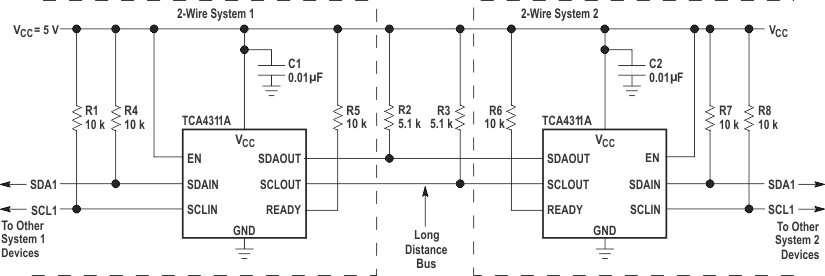
9.2.6 Repeater/Bus Extender Application
Users who wish to connect two 2-wire systems separated by a distance can do so by connecting two TCA4311A back-to-back, as shown in Figure 14. The I2C specification allows for 400 pF maximum bus capacitance, severely limiting the length of the bus. The SMBus specification places no restriction on bus capacitance, but the limited impedances of devices connected to the bus require systems to remain small if rise- and fall-time specifications are to be met. The strong pull-up and pull-down impedances of the TCA4311A are capable of meeting rise- and fall-time specifications for one nano-Farad of capacitance, thus allowing much more interconnect distance. In this situation, the differential ground voltage between the two systems may limit the allowed distance, because a valid logic low voltage with respect to the ground at one end of the system may violate the allowed VOL specification with respect to the ground at the other end. In addition, the connection circuitry offset voltages of the back-to-back TCA4311A add together, directly contributing to the same problem.
 Figure 14. Repeater/Bus Extender Schematic