ZHCSCU3C January 2014 – September 2019 TCA5013
PRODUCTION DATA.
- 1 特性
- 2 应用
- 3 说明
- 4 修订历史记录
- 5 Pin Configuration and Functions
-
6 Specifications
- 6.1 Absolute Maximum Ratings
- 6.2 Handling Ratings
- 6.3 Recommended Operating Conditions
- 6.4 Thermal Information
- 6.5 Electrical Characteristics—Power Supply and ESD
- 6.6 Electrical Characteristics—Card VCC
- 6.7 Electrical Characteristics—Card RST
- 6.8 Electrical Characteristics—Card CLK
- 6.9 Electrical Characteristics—Card Interface IO, C4 and C8
- 6.10 Electrical Characteristics—PRES
- 6.11 Electrical Characteristics—IOMC1 and IOMC2
- 6.12 Electrical Characteristics—CLKIN1 and CLKIN2
- 6.13 Electrical Characteristics—A0 and SHDN
- 6.14 Electrical Characteristics—INT
- 6.15 Electrical Characteristics—GPIO
- 6.16 Electrical Characteristics—SDA and SCL
- 6.17 Electrical Characteristics—Fault Condition Detection
- 6.18 I2C Interface Timing Requirements
- 6.19 I2C Interface Timing Characteristics
- 6.20 Synchronous Type 1 Card Activation Timing Characteristics
- 6.21 Synchronous Type 2 Card Activation Timing Characteristics
- 6.22 Card Deactivation Timing Characteristics
- 6.23 Typical Characteristics
- 7 Parameter Measurement Information
-
8 Detailed Description
- 8.1 Overview
- 8.2 Functional Block Diagram
- 8.3 Feature Description
- 8.4 Device Functional Modes
- 8.5 Programming
- 8.6 Register Maps
- 9 Application and Implementation
- 10Power Supply Recommendations
- 11Layout
- 12器件和文档支持
- 13机械、封装和可订购信息
8.4.4.2 Synchronous Type 1 Operating Mode
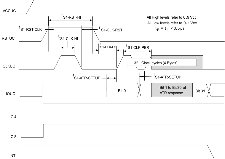
Synchronous type 1 operating mode is only supported on the user card interface. To enter synchronous operating mode, the user card interface goes through the synchronous type 1 activation sequence. Figure 4 shows the synchronous type 1 activation sequence.
CLKIN1 shall be low before the synchronous type 1 activation sequence is initiated. The following bit settings are required to initiate a synchronous type 1 activation sequence.
- ACTIVATION_TYPE (bit [6]; Reg 0x09) = 1
- CARD_TYPE (bit [7]; Reg 0x09) = 0
- START_SYNC (bit [0]; Reg 0x09) = 1
 Figure 4. Synchronous Type 1 Activation Sequence
 Once synchronous type 1 activation has been initiated, the following sequence of events occurs on the user card interface:
- VCCUC, RSTUC, CLKUC, C4, C8 and IOUC are all default low.
- VCC is applied to the VCCUC pin per the SET_VCC_UC bit (bit[7:6]; Reg 0x01).
- After VCC is stable RSTUC and CLKUC pulses are applied per tS1-RST-HI and tS1-CLK-HI defined in Table 2.
- After VCC is stable, the IOUC line is pulled up to VCC .
- After VCC is stable C4 and C8 reflect the value in their corresponding I2C register bits (bit[5] and bit[4]; Reg 0x09).
- RSTUC is held low while the CLKUC line starts oscillating with a frequency of ~40Khz (generated from internal oscillator).
- The IO line is sampled on the 32 rising or falling (based on bit[1]; Reg 0x09) edges of CLK and stored in the FIFO registers 0AH to 0DH.
- At the end of the 32nd CLK pulse, the CLKUC is held low and the CLKUC pin is controlled by the clock settings register (Reg 0x02).
- IOUC is connected to IOMC1 if IO_EN_UC bit (bit[5] Reg 0x01) is set to 1.
- INT_SYNC_COMPLETE bit (Bit[1]; REG 0x41) is set and the INT line is asserted low.
- IOMC1 shall stay pulled up to VDDI i.e. IOMC1 shall not be pulled low until INT is asserted.
- CLKIN1 shall toggle only after INT is asserted.
- RSTUC is controllable by I2C after INT is asserted.
Table 2. Synchronous Type 1 Card Activation Timing Characteristics
| MIN | TYP | MAX | UNIT | |
|---|---|---|---|---|
| tS1-RST-HI | 60 | 70 | 80 | µs |
| tS1-CLK-HI | 10 | 12.5 | 15 | µs |
| tS1-RST-CLK | 25 | 28 | 32 | µs |
| tS1-CLK-RST | 25 | 28 | 32 | µs |
| tS1-CLK-LO | 70 | 80 | 90 | µs |
| tS1-CLK-PER | 22.5 | 25 | 27.5 | µs |
| Duty cycle | 45 | 50 | 55 | % |