ZHCSRH9E April 2009 – January 2023 TCA6408A
PRODUCTION DATA
- 1 特性
- 2 应用
- 3 说明
- 4 Revision History
- 5 Pin Configuration and Functions
- 6 Specifications
- 7 Parameter Measurement Information
- 8 Detailed Description
- 9 Application and Implementation
- 10Power Supply Recommendations
- 11Layout
- 12Device and Documentation Support
封装选项
机械数据 (封装 | 引脚)
散热焊盘机械数据 (封装 | 引脚)
订购信息
9.2.2.1 Minimizing ICC When I/O is Used to Control LEDs
When the I/Os are used to control LEDs, normally they are connected to VCC through a resistor as shown in GUID-B0A4BE30-85A6-42AB-BEED-F3CC70F07A03.html#SCPS133IMG1020. The LED acts as a diode, so when the LED is off, the I/O VIN is about 1.2 V less than VCC. The ΔICC parameter in GUID-E4B3558E-EEC3-41D5-96D3-1E720DA96F11.html#GUID-E4B3558E-EEC3-41D5-96D3-1E720DA96F11 shows how ICC increases as VIN becomes lower than VCC. Designs that must minimize current consumption, such as battery power applications, should consider maintaining the I/O pins greater than or equal to VCC when the LED is off.
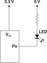
#SCPS133IMG9954 shows a high-value resistor in parallel with the LED. #SCPS133IMG5549 shows VCC less than the LED supply voltage by at least 1.2 V. Both of these methods maintain the I/O VIN at or above VCC and prevent additional supply current consumption when the LED is off.
 Figure 9-2 High-Value Resistor in Parallel With LED
 Figure 9-3 Device Supplied by a Low Voltage