ZHCSM91F May 2009 – January 2023 TCA6416A
PRODUCTION DATA
- 1 特性
- 2 应用
- 3 说明
- 4 Revision History
- 5 Pin Configuration and Functions
- 6 Specifications
- 7 Parameter Measurement Information
- 8 Detailed Description
- 9 Application and Implementation
- 10Power Supply Recommendations
- 11Layout
- 12Device and Documentation Support
- 13Mechanical, Packaging, and Orderable Information
封装选项
机械数据 (封装 | 引脚)
散热焊盘机械数据 (封装 | 引脚)
- RTW|24
订购信息
10.1 Power-On Reset Requirements
In the event of a glitch or data corruption, TCA6416A can be reset to its default conditions by using the power-on reset feature. Power-on reset requires that the device go through a power cycle to be completely reset. This reset also happens when the device is powered on for the first time in an application.
Ramping up the device VCCP before VCCI is recommended to prevent SDA from potentially being stuck LOW.
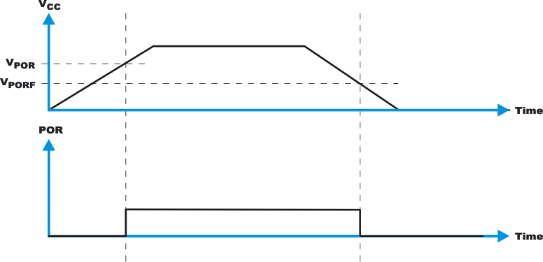
The two types of power-on reset are shown in #SCPS0691 and #SCPS0692.
 Figure 10-1 VCC is Lowered Below 0.2 V or 0 V and Then Ramped up to VCC
 Figure 10-2 VCC is Lowered Below the POR Threshold, Then Ramped Back up to VCC
Table 10-1 specifies the performance of the power-on reset feature for TCA6416A for both types of power-on reset.
| PARAMETER#SCPS139781#SCPS1397812 | MIN | TYP | MAX | UNIT | ||
|---|---|---|---|---|---|---|
| tFT | Fall rate | See #SCPS0691 | 0.1 | 2000 | ms | |
| tRT | Rise rate | See #SCPS0691 | 0.1 | 2000 | ms | |
| tTRR_GND | Time to re-ramp (when VCC drops to GND) | See #SCPS0691 | 1 | μs | ||
| tTRR_POR50 | Time to re-ramp (when VCC drops to VPOR_MIN – 50 mV) | See #SCPS0692 | 1 | μs | ||
| VCC_GH | Level that VCCP can glitch down to, but not cause a functional disruption when VCCX_GW = 1 μs | See #SCPS0693 | 1.2 | V | ||
| tGW | Glitch width that will not cause a functional disruption when VCCX_GH = 0.5 × VCCx | See #SCPS0693 | 10 | μs | ||
| VPORF | Voltage trip point of POR on falling VCC | 0.7 | V | |||
| VPORR | Voltage trip point of POR on rising VCC | 1.4 | V | |||
Glitches in the power supply can also affect the power-on reset performance of this device. The glitch width (VCC_GW) and height (VCC_GH) are dependent on each other. The bypass capacitance, source impedance, and device impedance are factors that affect power-on reset performance. #SCPS0693 and Table 10-1 provide more information on how to measure these specifications.
 Figure 10-3 Glitch Width and Glitch Height
VPOR is critical to the power-on reset. VPOR is the voltage level at which the reset condition is released and all the registers and the I2C/SMBus state machine are initialized to the default states. The value of VPOR differs based on the VCC being lowered to or from 0. #SCPS0694 and Table 10-1 provide more details on this specification.
 Figure 10-4 VPOR