ZHCS290G September 2009 – June 2018 TCA8418
PRODUCTION DATA.
- 1 特性
- 2 应用范围
- 3 说明
- 4 修订历史记录
- 5 Pin Configuration and Functions
-
6 Specifications
- 6.1 Absolute Maximum Ratings
- 6.2 ESD Ratings
- 6.3 Recommended Operating Conditions
- 6.4 Thermal Information
- 6.5 Electrical Characteristics
- 6.6 I2C Interface Timing Requirements
- 6.7 Reset Timing Requirements
- 6.8 Switching Characteristics
- 6.9 Keypad Switching Characteristics
- 6.10 Typical Characteristics
- 7 Parameter Measurement Information
-
8 Detailed Description
- 8.1 Overview
- 8.2 Functional Block Diagram
- 8.3 Feature Description
- 8.4 Device Functional Modes
- 8.5 Programming
- 8.6
Register Maps
- 8.6.1 Device Address
- 8.6.2
Control Register and Command Byte
- 8.6.2.1 Configuration Register (Address 0x01)
- 8.6.2.2 Interrupt Status Register, INT_STAT (Address 0x02)
- 8.6.2.3 Key Lock and Event Counter Register, KEY_LCK_EC (Address 0x03)
- 8.6.2.4 Key Event Registers (FIFO), KEY_EVENT_A–J (Address 0x04–0x0D)
- 8.6.2.5 Keypad Lock1 to Lock2 Timer Register, KP_LCK_TIMER (Address 0x0E)
- 8.6.2.6 Unlock1 and Unlock2 Registers, UNLOCK1/2 (Address 0x0F-0x10)
- 8.6.2.7 GPIO Interrupt Status Registers, GPIO_INT_STAT1–3 (Address 0x11–0x13)
- 8.6.2.8 GPIO Data Status Registers, GPIO_DAT_STAT1–3 (Address 0x14–0x16)
- 8.6.2.9 GPIO Data Out Registers, GPIO_DAT_OUT1–3 (Address 0x17–0x19)
- 8.6.2.10 GPIO Interrupt Enable Registers, GPIO_INT_EN1–3 (Address 0x1A–0x1C)
- 8.6.2.11 Keypad or GPIO Selection Registers, KP_GPIO1–3 (Address 0x1D–0x1F)
- 8.6.2.12 GPI Event Mode Registers, GPI_EM1–3 (Address 0x20–0x22)
- 8.6.2.13 GPIO Data Direction Registers, GPIO_DIR1–3 (Address 0x23–0x25)
- 8.6.2.14 GPIO Edge/Level Detect Registers, GPIO_INT_LVL1–3 (Address 0x26–0x28)
- 8.6.2.15 Debounce Disable Registers, DEBOUNCE_DIS1–3 (Address 0x29–0x2B)
- 8.6.2.16 GPIO pull-up Disable Register, GPIO_PULL1–3 (Address 0x2C–0x2E)
- 8.6.3 CAD Interrupt Errata
- 8.6.4 Overflow Errata
- 9 Application and Implementation
- 10Power Supply Recommendations
- 11Layout
- 12器件和文档支持
- 13机械、封装和可订购信息
7 Parameter Measurement Information

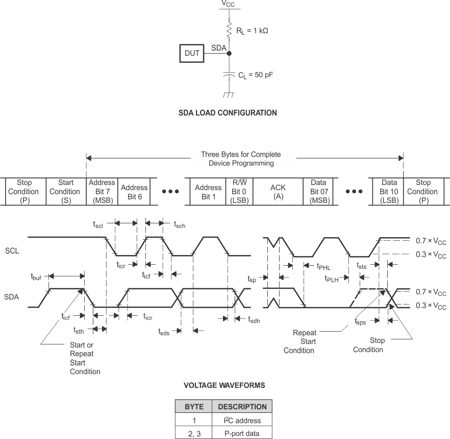
A. CL includes probe and jig capacitance. tocf is measured with CL of 10 pF or 400 pF.
B. All inputs are supplied by generators having the following characteristics: PRR ≤ 10 MHz, ZO = 50 Ω, tr/tf ≤ 30 ns.
C. All parameters and waveforms are not applicable to all devices.
Figure 16. I2C Interface Load Circuit And Voltage Waveforms 
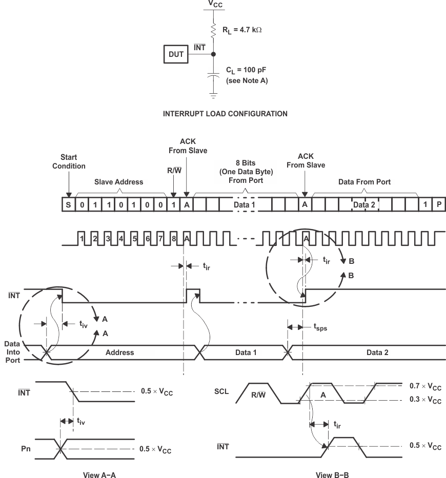
A. CL includes probe and jig capacitance.
B. All inputs are supplied by generators having the following characteristics: PRR ≤ 10 MHz, ZO = 50 Ω, tr/tf ≤ 30 ns.
C. All parameters and waveforms are not applicable to all devices.
Figure 17. Interrupt Load Circuit And Voltage Waveforms 
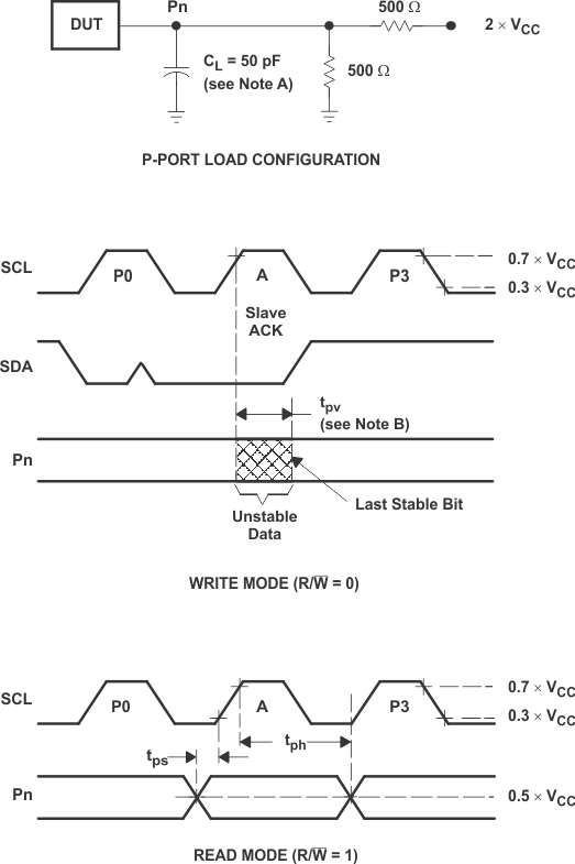
A. CL includes probe and jig capacitance.
B. tpv is measured from 0.7 × VCC on SCL to 50% I/O (Pn) output.
C. All inputs are supplied by generators having the following characteristics: PRR ≤ 10 MHz, ZO = 50 Ω, tr/tf ≤ 30 ns.
D. The outputs are measured one at a time, with one transition per measurement.
E. All parameters and waveforms are not applicable to all devices.
Figure 18. P Port Load Circuit And Timing Waveforms 
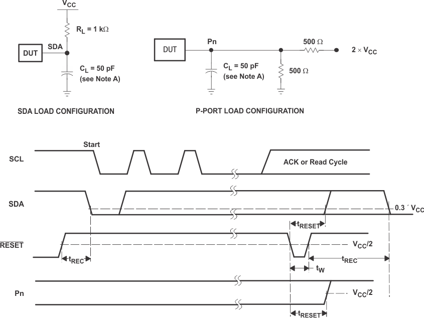
A. CL includes probe and jig capacitance.
B. All inputs are supplied by generators having the following characteristics: PRR ≤ 10 MHz, ZO = 50 Ω, tr/tf ≤ 30 ns.
C. The outputs are measured one at a time, with one transition per measurement.
D. I/Os are configured as inputs.
E. All parameters and waveforms are not applicable to all devices.
Figure 19. Reset Load Circuits And Voltage Waveforms