ZHCS290G September 2009 – June 2018 TCA8418
PRODUCTION DATA.
- 1 特性
- 2 应用范围
- 3 说明
- 4 修订历史记录
- 5 Pin Configuration and Functions
-
6 Specifications
- 6.1 Absolute Maximum Ratings
- 6.2 ESD Ratings
- 6.3 Recommended Operating Conditions
- 6.4 Thermal Information
- 6.5 Electrical Characteristics
- 6.6 I2C Interface Timing Requirements
- 6.7 Reset Timing Requirements
- 6.8 Switching Characteristics
- 6.9 Keypad Switching Characteristics
- 6.10 Typical Characteristics
- 7 Parameter Measurement Information
-
8 Detailed Description
- 8.1 Overview
- 8.2 Functional Block Diagram
- 8.3 Feature Description
- 8.4 Device Functional Modes
- 8.5 Programming
- 8.6
Register Maps
- 8.6.1 Device Address
- 8.6.2
Control Register and Command Byte
- 8.6.2.1 Configuration Register (Address 0x01)
- 8.6.2.2 Interrupt Status Register, INT_STAT (Address 0x02)
- 8.6.2.3 Key Lock and Event Counter Register, KEY_LCK_EC (Address 0x03)
- 8.6.2.4 Key Event Registers (FIFO), KEY_EVENT_A–J (Address 0x04–0x0D)
- 8.6.2.5 Keypad Lock1 to Lock2 Timer Register, KP_LCK_TIMER (Address 0x0E)
- 8.6.2.6 Unlock1 and Unlock2 Registers, UNLOCK1/2 (Address 0x0F-0x10)
- 8.6.2.7 GPIO Interrupt Status Registers, GPIO_INT_STAT1–3 (Address 0x11–0x13)
- 8.6.2.8 GPIO Data Status Registers, GPIO_DAT_STAT1–3 (Address 0x14–0x16)
- 8.6.2.9 GPIO Data Out Registers, GPIO_DAT_OUT1–3 (Address 0x17–0x19)
- 8.6.2.10 GPIO Interrupt Enable Registers, GPIO_INT_EN1–3 (Address 0x1A–0x1C)
- 8.6.2.11 Keypad or GPIO Selection Registers, KP_GPIO1–3 (Address 0x1D–0x1F)
- 8.6.2.12 GPI Event Mode Registers, GPI_EM1–3 (Address 0x20–0x22)
- 8.6.2.13 GPIO Data Direction Registers, GPIO_DIR1–3 (Address 0x23–0x25)
- 8.6.2.14 GPIO Edge/Level Detect Registers, GPIO_INT_LVL1–3 (Address 0x26–0x28)
- 8.6.2.15 Debounce Disable Registers, DEBOUNCE_DIS1–3 (Address 0x29–0x2B)
- 8.6.2.16 GPIO pull-up Disable Register, GPIO_PULL1–3 (Address 0x2C–0x2E)
- 8.6.3 CAD Interrupt Errata
- 8.6.4 Overflow Errata
- 9 Application and Implementation
- 10Power Supply Recommendations
- 11Layout
- 12器件和文档支持
- 13机械、封装和可订购信息
8.3.2 Keypad Lock/Unlock
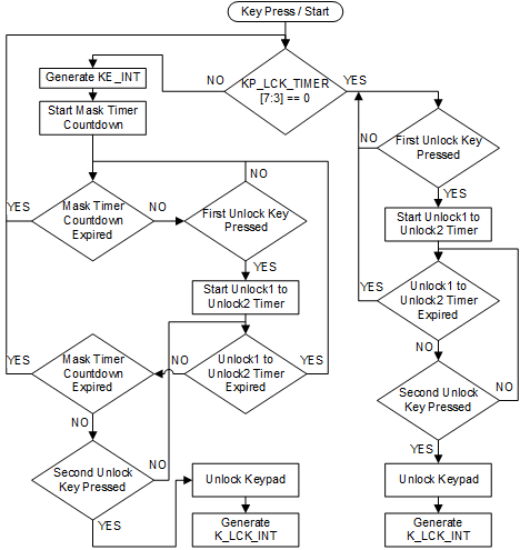
This user can lock the keypad through the lock/unlock feature in this device. Once the keypad is locked by setting BIT6 in KEY_LCK_EC, it can prevent the generation of key event interrupts and recorded key events. The unlock keys can be programmed with any value of the keys in the keypad matrix or any general purpose input (GPI) values that are part of the Key Event Table. When the keypad lock interrupt mask timer is non-zero, the user will need to press two specific keys before an keylock interrupt is generated or keypad events are recorded. A key event interrupt is generated the first time a user presses any key. This first interrupt can be used to turn on an LCD and display the unlock message. The processor will then read the lock status register to see if the keypad is unlocked. The next interrupt (keylock interrupt) will not be generated unless both unlock keys sequences are correct. If correct Unlock keys are not pressed before the mask timer expires, the state machine will start over again.
The recommended procedure to lock the keypad is to do the following
- Determine which keys will be used for the unlock sequence. The key value from the Key Event Tables needs to be entered into the UNLOCK1 and UNLOCK2 registers.
- The UNLOCK1 to UNLOCK2 timer duration must be set by entering the desired seconds (valid range is 0 to 7 seconds) into bits [2:0] of the KP_LCK_TMR register.
- If an interrupt mask is desired (see Keypad Lock Interrupt Mask Timer), then the desired interrupt mask duration (valid range is 0 to 31 seconds) must be entered into bits [7:3] of the KP_LCK_TMR register.
- When the host is ready to lock the keypad, a 1 is to be written to the K_LCK_EN bit (BIT6) in the KEY_LCK_EC register. This will lock the keypad.
- If the host wishes to manually unlock the keypad, writing a '0' to the K_LCK_EN bit (BIT6) in the KEY_LCK_EC register will unlock the keypad.
 Figure 20. Keypad Lock Flowchart