ZHCS290G September 2009 – June 2018 TCA8418
PRODUCTION DATA.
- 1 特性
- 2 应用范围
- 3 说明
- 4 修订历史记录
- 5 Pin Configuration and Functions
-
6 Specifications
- 6.1 Absolute Maximum Ratings
- 6.2 ESD Ratings
- 6.3 Recommended Operating Conditions
- 6.4 Thermal Information
- 6.5 Electrical Characteristics
- 6.6 I2C Interface Timing Requirements
- 6.7 Reset Timing Requirements
- 6.8 Switching Characteristics
- 6.9 Keypad Switching Characteristics
- 6.10 Typical Characteristics
- 7 Parameter Measurement Information
-
8 Detailed Description
- 8.1 Overview
- 8.2 Functional Block Diagram
- 8.3 Feature Description
- 8.4 Device Functional Modes
- 8.5 Programming
- 8.6
Register Maps
- 8.6.1 Device Address
- 8.6.2
Control Register and Command Byte
- 8.6.2.1 Configuration Register (Address 0x01)
- 8.6.2.2 Interrupt Status Register, INT_STAT (Address 0x02)
- 8.6.2.3 Key Lock and Event Counter Register, KEY_LCK_EC (Address 0x03)
- 8.6.2.4 Key Event Registers (FIFO), KEY_EVENT_A–J (Address 0x04–0x0D)
- 8.6.2.5 Keypad Lock1 to Lock2 Timer Register, KP_LCK_TIMER (Address 0x0E)
- 8.6.2.6 Unlock1 and Unlock2 Registers, UNLOCK1/2 (Address 0x0F-0x10)
- 8.6.2.7 GPIO Interrupt Status Registers, GPIO_INT_STAT1–3 (Address 0x11–0x13)
- 8.6.2.8 GPIO Data Status Registers, GPIO_DAT_STAT1–3 (Address 0x14–0x16)
- 8.6.2.9 GPIO Data Out Registers, GPIO_DAT_OUT1–3 (Address 0x17–0x19)
- 8.6.2.10 GPIO Interrupt Enable Registers, GPIO_INT_EN1–3 (Address 0x1A–0x1C)
- 8.6.2.11 Keypad or GPIO Selection Registers, KP_GPIO1–3 (Address 0x1D–0x1F)
- 8.6.2.12 GPI Event Mode Registers, GPI_EM1–3 (Address 0x20–0x22)
- 8.6.2.13 GPIO Data Direction Registers, GPIO_DIR1–3 (Address 0x23–0x25)
- 8.6.2.14 GPIO Edge/Level Detect Registers, GPIO_INT_LVL1–3 (Address 0x26–0x28)
- 8.6.2.15 Debounce Disable Registers, DEBOUNCE_DIS1–3 (Address 0x29–0x2B)
- 8.6.2.16 GPIO pull-up Disable Register, GPIO_PULL1–3 (Address 0x2C–0x2E)
- 8.6.3 CAD Interrupt Errata
- 8.6.4 Overflow Errata
- 9 Application and Implementation
- 10Power Supply Recommendations
- 11Layout
- 12器件和文档支持
- 13机械、封装和可订购信息
8.5.1 I2C Interface
The TCA8418 has a standard bidirectional I2C interface that is controlled by a master device in order to be configured or read the status of this device. Each slave on the I2C bus has a specific device address to differentiate between other slave devices that are on the same I2C bus. Many slave devices will require configuration upon startup to set the behavior of the device. This is typically done when the master accesses internal register maps of the slave, which have unique register addresses. A device can have one or multiple registers where data is stored, written, or read.
The physical I2C interface consists of the serial clock (SCL) and serial data (SDA) lines. Both SDA and SCL lines must be connected to VCC through a pull-up resistor. The size of the pull-up resistor is determined by the amount of capacitance on the I2C lines. (For further details, refer to I2C pull-up Resistor Calculation (SLVA689).) Data transfer may be initiated only when the bus is idle. A bus is considered idle if both SDA and SCL lines are high after a STOP condition.
The following is the general procedure for a master to access a slave device:
- If a master wants to send data to a slave:
- Master-transmitter sends a START condition and addresses the slave-receiver.
- Master-transmitter sends data to slave-receiver.
- Master-transmitter terminates the transfer with a STOP condition.
- If a master wants to receive or read data from a slave:
- Master-receiver sends a START condition and addresses the slave-transmitter.
- Master-receiver sends the requested register to read to slave-transmitter.
- Master-receiver receives data from the slave-transmitter.
- Master-receiver terminates the transfer with a STOP condition.
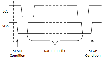
 Figure 21. Definition of Start and Stop Conditions
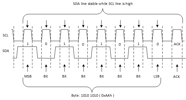
  Figure 22. Bit Transfer