SCPS222C May 2010 – October 2015 TCA8418E
PRODUCTION DATA.
- 1 Features
- 2 Applications
- 3 Description
- 4 Revision History
- 5 Pin Configuration and Functions
-
6 Specifications
- 6.1 Absolute Maximum Ratings
- 6.2 ESD Ratings
- 6.3 Recommended Operating Conditions
- 6.4 Thermal Information
- 6.5 Electrical Characteristics
- 6.6 I2C Interface Timing Requirements
- 6.7 Reset Timing Requirements for Standard Mode, Fast Mode, Fast Mode Plus (FM+) I2C Bus
- 6.8 Switching Characteristics for Standard Mode, Fast Mode, Fast Mode Plus (FM+) I2C Bus
- 6.9 Keypad Switching Characteristics for Standard Mode, Fast Mode, Fast Mode Plus (FM+) I2C Bus
- 6.10 Typical Characteristics
- 7 Parameter Measurement Information
-
8 Detailed Description
- 8.1 Overview
- 8.2 Functional Block Diagram
- 8.3 Feature Description
- 8.4 Device Functional Modes
- 8.5 Programming
- 8.6
Register Maps
- 8.6.1 Device Address
- 8.6.2
Control Register and Command Byte
- 8.6.2.1 Configuration Register (Address 0x01)
- 8.6.2.2 Interrupt Status Register, INT_STAT (Address 0x02)
- 8.6.2.3 Key Lock and Event Counter Register, KEY_LCK_EC (Address 0x03)
- 8.6.2.4 Key Event Registers (FIFO), KEY_EVENT_A-J (Address 0x04-0x0D)
- 8.6.2.5 Keypad Lock1 to Lock2 Timer Register, KP_LCK_TIMER (Address 0x0E)
- 8.6.2.6 Unlock1 and Unlock2 Registers, UNLOCK1/2 (Address 0x0F-0x10)
- 8.6.2.7 GPIO Interrupt Status Registers, GPIO_INT_STAT1-3 (Address 0x11-0x13)
- 8.6.2.8 GPIO Data Status Registers, GPIO_DAT_STAT1-3 (Address 0x14-0x16)
- 8.6.2.9 GPIO Data Out Registers, GPIO_DAT_OUT1-3 (Address 0x17-0x19)
- 8.6.2.10 GPIO Interrupt Enable Registers, GPIO_INT_EN1-3 (Address 0x1A-0x1C)
- 8.6.2.11 Keypad or GPIO Selection Registers, KP_GPIO1-3 (Address 0x1D-0x1F)
- 8.6.2.12 GPI Event Mode Registers, GPI_EM1-3 (Address 0x20-0x22)
- 8.6.2.13 GPIO Data Direction Registers, GPIO_DIR1-3 (Address 0x23-0x25)
- 8.6.2.14 GPIO Edge/Level Detect Registers, GPIO_INT_LVL1-3 (Address 0x26-0x28)
- 8.6.2.15 Debounce Disable Registers, DEBOUNCE_DIS1-3 (Address 0x29-0x2B)
- 8.6.2.16 GPIO Pullup Disable Register, GPIO_PULL1-3 (Address 0x2C-0x2E)
- 9 Application and Implementation
- 10Power Supply Recommendations
- 11Layout
- 12Device and Documentation Support
- 13Mechanical, Packaging, and Orderable Information
5 Pin Configuration and Functions
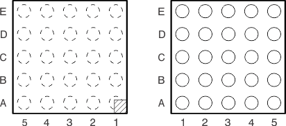
YFP Package
25-Pin DSBGA
Laser Marking and Bump Views

Pin Assignments
| E | INT | GND | COL5 | COL0 | ROW3 |
| D | SCL | COL9 | COL4 | ROW0 | ROW4 |
| C | SDA | COL8 | COL3 | ROW1 | ROW5 |
| B | VCC | COL7 | COL2 | CAD_INT | ROW6 |
| A | RESET | COL6 | COL1 | ROW2 | ROW7 |
| 5 | 4 | 3 | 2 | 1 |
Pin Functions
| PIN | I/O | DESCRIPTION | |
|---|---|---|---|
| NO. | NAME | ||
| A1 | ROW7 | I/O | GPIO or row 7 in keypad matrix. If unused, connect to VCC through a pullup resistor. |
| A2 | ROW2 | I/O | GPIO or row 2 in keypad matrix. If unused, connect to VCC through a pullup resistor. |
| A3 | COL1 | I/O | GPIO or column 1 in keypad matrix. If unused, connect to VCC through a pullup resistor. |
| A4 | COL6 | I/O | GPIO or column 6 in keypad matrix. If unused, connect to VCC through a pullup resistor. |
| A5 | RESET | I | Active-low reset input. Connect to VCC through a pullup resistor, if no active connection is used. |
| B1 | ROW6 | I/O | GPIO or row 6 in keypad matrix |
| B2 | CAD_INT | O | Active-low interrupt hardware output for 3-key simultaneous press-event. Open drain structure. Connect to VCC through a pullup resistor. |
| B3 | COL2 | I/O | GPIO or column 2 in keypad matrix. If unused, connect to VCC through a pullup resistor. |
| B4 | COL7 | I/O | GPIO or column 7 in keypad matrix. If unused, connect to VCC through a pullup resistor. |
| B5 | VCC | - | Supply voltage of 1.65 V to 3.6 V |
| C1 | ROW5 | I/O | GPIO or row 5 in keypad matrix. If unused, connect to VCC through a pullup resistor. |
| C2 | ROW1 | I/O | GPIO or row 1 in keypad matrix. If unused, connect to VCC through a pullup resistor. |
| C3 | COL3 | I/O | GPIO or column 3 in keypad matrix. If unused, connect to VCC through a pullup resistor. |
| C4 | COL8 | I/O | GPIO or column 8 in keypad matrix. If unused, connect to VCC through a pullup resistor. |
| C5 | SDA | I/O | Serial data bus. Connect to VCC through a pullup resistor. |
| D1 | ROW4 | I/O | GPIO or row 4 in keypad matrix. If unused, connect to VCC through a pullup resistor. |
| D2 | ROW0 | I/O | GPIO or row 0 in keypad matrix. If unused, connect to VCC through a pullup resistor. |
| D3 | COL4 | I/O | GPIO or column 4 in keypad matrix. If unused, connect to VCC through a pullup resistor. |
| D4 | COL9 | I/O | GPIO or column 9 in keypad matrix. If unused, connect to VCC through a pullup resistor. |
| D5 | SCL | I | Serial clock bus. Connect to VCC through a pullup resistor. |
| E1 | ROW3 | I/O | GPIO or row 3 in keypad matrix. If unused, connect to VCC through a pullup resistor. |
| E2 | COL0 | I/O | GPIO or column 0 in keypad matrix. If unused, connect to VCC through a pullup resistor. |
| E3 | COL5 | I/O | GPIO or column 5 in keypad matrix. If unused, connect to VCC through a pullup resistor. |
| E4 | GND | – | Ground |
| E5 | INT | O | Active-low interrupt output. Open drain structure. Connect to VCC through a pullup resistor. |