ZHCS352E August 2011 – October 2024 TCA9509
PRODUCTION DATA
- 1
- 1 特性
- 2 应用
- 3 说明
- 4 Pin Configuration and Functions
- 5 Specifications
- 6 Parameter Measurement Information
- 7 Detailed Description
- 8 Application and Implementation
- 9 Power Supply Recommendations
- 10Layout
- 11Device and Documentation Support
- 12Revision History
- 13Mechanical, Packaging, and Orderable Information
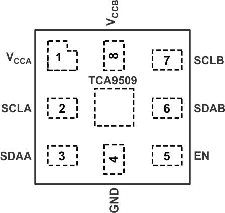
4 Pin Configuration and Functions
 Figure 4-1 RVH Package,8-Pin X2QFN,Top View
 Figure 4-2 DGK Package,8-Pin VSSOP,Top View
Table 4-1 Pin Functions
| PIN | I/O | DESCRIPTION | |
|---|---|---|---|
| NAME | NO. | ||
| VCCA | 1 | Supply | A-side supply voltage (0.9 V to 5.5 V) |
| SCLA | 2 | I/O | Serial clock bus, A side. |
| SDAA | 3 | I/O | Serial data bus, A side. |
| GND | 4 | Supply | Supply ground |
| EN | 5 | Input | Active-high repeater enable input |
| SDAB | 6 | I/O | Serial data bus, B side. Connect to VCCB through a pull-up resistor. |
| SCLB | 7 | I/O | Serial clock bus, B side. Connect to VCCB through a pull-up resistor. |
| VCCB | 8 | Supply | B-side and device supply voltage (2.7 V to 5.5 V) |
| Thermal Attach Pad | - | - | Thermal Attach Pad is not electrically connected and it is recommended to be attached to GND for best thermal performance. This is for the RVH package only. |