ZHCSIF1A June   2018  – February 2022 TCA9517-Q1

PRODUCTION DATA  

  1. 特性
  2. 应用
  3. 说明
  4. Revision History
  5. 说明(续)
  6. Pin Configuration and Functions
  7. Specifications
    1. 7.1 Absolute Maximum Ratings
    2. 7.2 ESD Ratings
    3. 7.3 Recommended Operating Conditions
    4. 7.4 Thermal Information
    5. 7.5 Electrical Characteristics
    6. 7.6 Timing Requirements
    7. 7.7 I2C Interface Switching Characteristics
    8. 7.8 Typical Characteristics
  8. Parameter Measurement Information
  9. Detailed Description
    1. 9.1 Overview
    2. 9.2 Functional Block Diagram
    3. 9.3 Feature Description
      1. 9.3.1 Two-Channel Bidirectional Buffer
      2. 9.3.2 Active-High Repeater-Enable Input
      3. 9.3.3 VOL B-Side Offset Voltage
      4. 9.3.4 Standard Mode and Fast Mode Support
      5. 9.3.5 Clock Stretching Support
    4. 9.4 Device Functional Modes
  10. 10Application and Implementation
    1. 10.1 Application Information
    2. 10.2 Typical Application
      1. 10.2.1 Design Requirements
      2. 10.2.2 Detailed Design Procedure
        1. 10.2.2.1 Clock Stretching Support
        2. 10.2.2.2 VILC and Pullup Resistor Sizing
      3. 10.2.3 Application Curve
  11. 11Power Supply Recommendations
  12. 12Layout
    1. 12.1 Layout Guidelines
    2. 12.2 Layout Example
  13. 13Device and Documentation Support
    1. 13.1 Device Support
    2. 13.2 Receiving Notification of Documentation Updates
    3. 13.3 支持资源
    4. 13.4 Trademarks
    5. 13.5 Electrostatic Discharge Caution
    6. 13.6 术语表

封装选项

机械数据 (封装 | 引脚)
散热焊盘机械数据 (封装 | 引脚)
订购信息

VILC and Pullup Resistor Sizing

For the TCA9517-Q1 to function correctly, all devices on the B-side must be able to pull the B-side below the voltage input low contention level (VILC). This means that the VOL of any device on the B-side must be below
0.4 V.

VOL of a device can be adjusted by changing the IOL through the device which is set by the pull-up resistance value. The pull-up resistance on the B-side must be carefully selected to ensure that logic levels will be transferred correctly to the A-side.
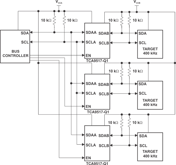
GUID-E9B9D537-B65A-4B93-AC0D-0BFF96424FEC-low.gifFigure 10-2 Typical Star Application

Multiple A sides of TCA9517-Q1s can be connected in a star configuration, allowing all nodes to communicate with each other.

GUID-BFE78933-D59C-413D-80BB-CBD35A6AEE2D-low.gifFigure 10-3 Typical Series Application

To further extend the I2C bus for long traces/cables, multiple TCA9517-Q1s can be connected in series as long as the A-side is connected to the B-side. I2C bus target devices can be connected to any of the bus segments. The number of devices that can be connected in series is limited by repeater delay/time-of-flight considerations on the maximum bus speed requirements.

GUID-79FD8179-0FF4-44B6-881B-590A4EBBE522-low.gifFigure 10-4 Bus A (0.9 V to 5.25 V Bus) Waveform
GUID-9A068D3F-C9B9-4F1F-A190-F3B0537A5F76-low.gifFigure 10-5 Bus B (2.7 V to 5.25 V Bus) Waveform