ZHCSAM0D December 2012 – September 2024 TCA9517A
PRODUCTION DATA
- 1
- 1 特性
- 2 应用
- 3 说明
- 4 Pin Configuration and Functions
- 5 Specifications
- 6 Parameter Measurement Information
- 7 Detailed Description
- 8 Application and Implementation
- 9 Power Supply Recommendations
- 10Layout
- 11Device and Documentation Support
- 12Revision History
- 13Mechanical, Packaging, and Orderable Information
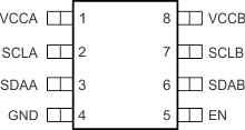
4 Pin Configuration and Functions
 Figure 4-1 DGK Package, 8-Pin VSSOP
(Top View)
 Figure 4-2 D Packages, 8-Pin SOIC
Top View
 Figure 4-3 DGK Package, 8-Pin
VSSOP
Figure 4-3 DGK Package, 8-Pin
VSSOPTop View
Table 4-1 Pin Functions
| PIN | TYPE | DESCRIPTION | |
|---|---|---|---|
| NO. | NAME | ||
| 1 | VCCA | Supply | A-side supply voltage (0.9 V to 5.5 V) |
| 2 | SCLA | Input/Output | Serial clock bus, A-side. Connect to VCCA through a pull-up resistor. If unused, connect directly to ground. |
| 3 | SDAA | Input/Output | Serial data bus, A-side. Connect to VCCA through a pull-up resistor. If unused, connect directly to ground. |
| 4 | GND | Ground | Ground |
| 5 | EN | Input | Active-high repeater enable input |
| 6 | SDAB | Input/Output | Serial data bus, B-side. Connect to VCCB through a pull-up resistor. If unused, connect directly to ground. |
| 7 | SCLB | Input/Output | Serial clock bus, B-side. Connect to VCCB through a pull-up resistor. If unused, connect directly to ground. |
| 8 | VCCB | Supply | B-side and device supply voltage (2.7 V to 5.5 V) |