ZHCSCR9C September   2014  – February 2017 TCA9534A

PRODUCTION DATA.  

  1. 特性
  2. 应用
  3. 说明
    1.     Device Images
      1.      简化的原理图
  4. 修订历史记录
  5. Pin Configuration and Functions
  6. Specifications
    1. 6.1 Absolute Maximum Ratings
    2. 6.2 Handling Ratings
    3. 6.3 Recommended Operating Conditions
    4. 6.4 Thermal Information
    5. 6.5 Electrical Characteristics
    6. 6.6 I2C Interface Timing Requirements
    7. 6.7 Switching Characteristics
    8. 6.8 Typical Characteristics
  7. Parameter Measurement Information
  8. Detailed Description
    1. 8.1 Overview
    2. 8.2 Functional Block Diagram
    3. 8.3 Feature Description
      1. 8.3.1 I/O Port
      2. 8.3.2 Interrupt Output (INT)
    4. 8.4 Device Functional Modes
      1. 8.4.1 Power-On Reset
    5. 8.5 Programming
      1. 8.5.1 I2C Interface
    6. 8.6 Register Maps
      1. 8.6.1 Device Address
      2. 8.6.2 Control Register and Command Byte
      3. 8.6.3 Register Descriptions
        1. 8.6.3.1 Bus Transactions
          1. 8.6.3.1.1 Writes
          2. 8.6.3.1.2 Reads
  9. Application and Implementation
    1. 9.1 Application Information
    2. 9.2 Typical Application
      1. 9.2.1 Design Requirements
        1. 9.2.1.1 Calculating Junction Temperature and Power Dissipation
        2. 9.2.1.2 Minimizing ICC When I/Os Control LEDs
      2. 9.2.2 Detailed Design Procedure
      3. 9.2.3 Application Curves
  10. 10Power Supply Recommendations
    1. 10.1 Power-On Reset Requirements
  11. 11Layout
    1. 11.1 Layout Guidelines
    2. 11.2 Layout Example
  12. 12器件和文档支持
    1. 12.1 相关文档 
    2. 12.2 接收文档更新通知
    3. 12.3 社区资源
    4. 12.4 商标
    5. 12.5 静电放电警告
    6. 12.6 Glossary
  13. 13机械、封装和可订购信息

封装选项

机械数据 (封装 | 引脚)
散热焊盘机械数据 (封装 | 引脚)
订购信息

Typical Application

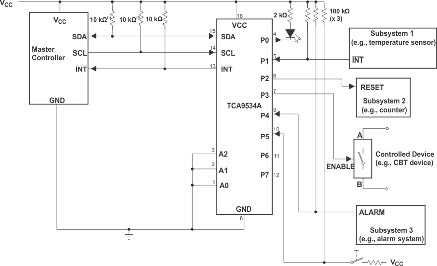
TCA9534A typ_app_cps198.gif
The SCL and SDA pins must be tied directly to VCC because if SCL and SDA are tied to an auxiliary power supply that can be powered on while VCC is powered off, then the supply current, ICC, increases as a result.
Device address is configured as 0111000 for this example.
P0, P2, and P3 are configured as outputs.
P1, P4, and P5 are configured as inputs.
P6 and P7 are not used and must be configured as outputs.
Figure 33. Application Schematic