ZHCSCR9C September 2014 – February 2017 TCA9534A
PRODUCTION DATA.
- 1 特性
- 2 应用
- 3 说明
- 4 修订历史记录
- 5 Pin Configuration and Functions
- 6 Specifications
- 7 Parameter Measurement Information
- 8 Detailed Description
- 9 Application and Implementation
- 10Power Supply Recommendations
- 11Layout
- 12器件和文档支持
- 13机械、封装和可订购信息
封装选项
机械数据 (封装 | 引脚)
散热焊盘机械数据 (封装 | 引脚)
- DW|16
订购信息
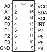
5 Pin Configuration and Functions
PW and DW Package
16-Pin TSSOP and SOIC
Top View

Pin Functions
| PIN | I/O | DESCRIPTION | |
|---|---|---|---|
| NO. | NAME | ||
| 1 | A0 | I | Address input. Connect directly to VCC or ground |
| 2 | A1 | I | Address input. Connect directly to VCC or ground |
| 3 | A2 | I | Address input. Connect directly to VCC or ground |
| 4 | P0 | I/O | P-port input-output. Push-pull design structure. At power on, P0 is configured as an input |
| 5 | P1 | I/O | P-port input-output. Push-pull design structure. At power on, P1 is configured as an input |
| 6 | P2 | I/O | P-port input-output. Push-pull design structure. At power on, P2 is configured as an input |
| 7 | P3 | I/O | P-port input-output. Push-pull design structure. At power on, P3 is configured as an input |
| 8 | GND | — | Ground |
| 9 | P4 | I/O | P-port input-output. Push-pull design structure. At power on, P4 is configured as an input |
| 10 | P5 | I/O | P-port input-output. Push-pull design structure. At power on, P5 is configured as an input |
| 11 | P6 | I/O | P-port input-output. Push-pull design structure. At power on, P6 is configured as an input |
| 12 | P7 | I/O | P-port input-output. Push-pull design structure. At power on, P7 is configured as an input |
| 13 | INT | O | Interrupt output. Connect to VCC through a pull-up resistor |
| 14 | SCL | I | Serial clock bus. Connect to VCC through a pull-up resistor |
| 15 | SDA | I/O | Serial data bus. Connect to VCC through a pull-up resistor |
| 16 | VCC | — | Supply voltage |