ZHCSEZ2D January 2014 – October 2021 TCA9539-Q1
PRODUCTION DATA
- 1 特性
- 2 应用
- 3 说明
- 4 Revision History
- 5 Pin Configuration and Functions
- 6 Specifications
- 7 Parameter Measurement Information
- 8 Detailed Description
- 9 Power Supply Recommendations
- 10Layout
- 11Device and Documentation Support
8.6.3.1.1 Writes
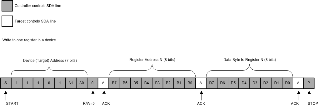
To write on the I2C bus, the controller sends a START condition on the bus with the address of the target, as well as the last bit (the R/ W bit) set to 0, which signifies a write. After the target sends the acknowledge bit, the controller then sends the register address of the register to which it wishes to write. The target acknowledges again, letting the controller know it is ready. After this, the controller starts sending the register data to the target until the controller has sent all the data necessary (which is sometimes only a single byte), and the controller terminates the transmission with a STOP condition.
See the Section 8.6.2 section to see list of the TCA9539-Q1s internal registers and a description of each one.
Figure 8-7 shows an example of writing a single byte to a target register.
 Figure 8-7 Write to
Register
Figure 8-7 Write to
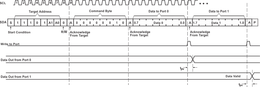
RegisterFigure 8-9 shows the Write to the Polarity Inversion Register.
 Figure 8-8 Write to
the Polarity Inversion Register
Figure 8-8 Write to
the Polarity Inversion RegisterFigure 8-9 shows the Write to Output Port Registers
 Figure 8-9 Write to
Output Port Registers