SCPS202C October 2009 – May 2016 TCA9539
PRODUCTION DATA.
- 1 Features
- 2 Applications
- 3 Description
- 4 Revision History
- 5 Pin Configuration and Functions
- 6 Specifications
- 7 Parameter Measurement Information
- 8 Detailed Description
- 9 Application and Implementation
- 10Power Supply Recommendations
- 11Layout
- 12Device and Documentation Support
- 13Mechanical, Packaging, and Orderable Information
封装选项
机械数据 (封装 | 引脚)
散热焊盘机械数据 (封装 | 引脚)
订购信息
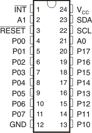
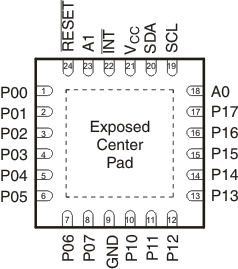
5 Pin Configuration and Functions
PW Package
24-Pins TSSOP
Top View

RTW, RGE Package
24-Pins WQFN, VQFN
Top View

Pin Functions
| NAME | NO. | I/O | DESCRIPTION | |
|---|---|---|---|---|
| TSSOP (PW) |
QFN (RTW, RGE) |
|||
| A0 | 21 | 18 | I | Address input. Connect directly to VCC or ground |
| A1 | 2 | 23 | I | Address input. Connect directly to VCC or ground |
| GND | 12 | 9 | — | Ground |
| INT | 1 | 22 | O | Interrupt open-drain output. Connect to VCC through a pull-up resistor |
| RESET | 3 | 24 | I | Active-low reset input. Connect to VCC through a pull-up resistor if no active connection is used |
| P00 | 4 | 1 | I/O | P-port input-output. Push-pull design structure. At power on, P00 is configured as an input |
| P01 | 5 | 2 | I/O | P-port input-output. Push-pull design structure. At power on, P01 is configured as an input |
| P02 | 6 | 3 | I/O | P-port input-output. Push-pull design structure. At power on, P02 is configured as an input |
| P03 | 7 | 4 | I/O | P-port input-output. Push-pull design structure. At power on, P03 is configured as an input |
| P04 | 8 | 5 | I/O | P-port input-output. Push-pull design structure. At power on, P04 is configured as an input |
| P05 | 9 | 6 | I/O | P-port input-output. Push-pull design structure. At power on, P05 is configured as an input |
| P06 | 10 | 7 | I/O | P-port input-output. Push-pull design structure. At power on, P06 is configured as an input |
| P07 | 11 | 8 | I/O | P-port input-output. Push-pull design structure. At power on, P07 is configured as an input |
| P10 | 13 | 10 | I/O | P-port input-output. Push-pull design structure. At power on, P10 is configured as an input |
| P11 | 14 | 11 | I/O | P-port input-output. Push-pull design structure. At power on, P11 is configured as an input |
| P12 | 15 | 12 | I/O | P-port input-output. Push-pull design structure. At power on, P12 is configured as an input |
| P13 | 16 | 13 | I/O | P-port input-output. Push-pull design structure. At power on, P13 is configured as an input |
| P14 | 17 | 14 | I/O | P-port input-output. Push-pull design structure. At power on, P14 is configured as an input |
| P15 | 18 | 15 | I/O | P-port input-output. Push-pull design structure. At power on, P15 is configured as an input |
| P16 | 19 | 16 | I/O | P-port input-output. Push-pull design structure. At power on, P16 is configured as an input |
| P17 | 20 | 17 | I/O | P-port input-output. Push-pull design structure. At power on, P17 is configured as an input |
| SCL | 22 | 19 | I | Serial clock bus. Connect to VCC through a pull-up resistor |
| SDA | 23 | 20 | I/O | Serial data bus. Connect to VCC through a pull-up resistor |
| VCC | 24 | 21 | — | Supply voltage |