ZHCSC52D January   2014  – November 2019 TCA9545A

PRODUCTION DATA.  

  1. 特性
  2. 应用
  3. 说明
    1.     Device Images
      1.      简化的应用示意图
  4. 修订历史记录
  5. Pin Configuration and Functions
    1.     Pin Functions
  6. Specifications
    1. 6.1 Absolute Maximum Ratings
    2. 6.2 ESD Ratings
    3. 6.3 Recommended Operating Conditions
    4. 6.4 Thermal Information
    5. 6.5 Electrical Characteristics
    6. 6.6 I2C Interface Timing Requirements
    7. 6.7 Switching Characteristics
    8. 6.8 Interrupt and Reset Timing Requirements
    9. 6.9 Typical Characteristics
  7. Parameter Measurement Information
  8. Detailed Description
    1. 8.1 Overview
    2. 8.2 Functional Block Diagram
    3. 8.3 Feature Description
    4. 8.4 Device Functional Modes
      1. 8.4.1 RESET Input
      2. 8.4.2 Power-On Reset
    5. 8.5 Programming
      1. 8.5.1 I2C Interface
    6. 8.6 Control Register
      1. 8.6.1 Device Address
      2. 8.6.2 Control Register Description
      3. 8.6.3 Control Register Definition
      4. 8.6.4 Interrupt Handling
  9. Application and Implementation
    1. 9.1 Application Information
    2. 9.2 Typical Application
      1. 9.2.1 Design Requirements
      2. 9.2.2 Detailed Design Procedure
      3. 9.2.3 TCA9545A Application Curves
  10. 10Power Supply Recommendations
    1. 10.1 Power-On Reset Requirements
  11. 11Layout
    1. 11.1 Layout Guidelines
    2. 11.2 Layout Example
  12. 12器件和文档支持
    1. 12.1 接收文档更新通知
    2. 12.2 支持资源
    3. 12.3 商标
    4. 12.4 静电放电警告
    5. 12.5 Glossary
  13. 13机械、封装和可订购信息

封装选项

机械数据 (封装 | 引脚)
散热焊盘机械数据 (封装 | 引脚)
订购信息

Typical Application

A typical application of the TCA9545A will contain anywhere from 1 to 5 separate data pull-up voltages, VDPUX , one for the master device (VDPUM) and one for each of the selectable slave channels (VDPU0 – VDPU3). In the event where the master device and all slave devices operate at the same voltage, then the pass voltage, Vpass = VDPUX. Once the maximum Vpass is known, Vcc can be selected easily using Figure 17. In an application where voltage translation is necessary, additional design requirements must be considered (See Design Requirements).

Figure 16 shows an application in which the TCA9545A can be used.
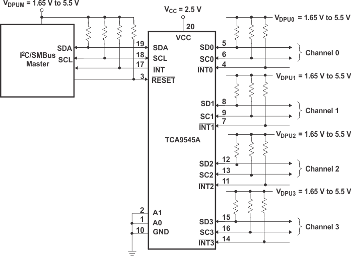
TCA9545A typ_app_cps204.gifFigure 16. TCA9545A Typical Application Schematic