ZHCS616E March 2012 – February 2017 TCA9554
PRODUCTION DATA.
- 1 特性
- 2 应用
- 3 说明
- 4 修订历史记录
- 5 Pin Configuration and Functions
- 6 Specifications
- 7 Parameter Measurement Information
- 8 Detailed Description
- 9 Application and Implementation
- 10Power Supply Recommendations
- 11Layout
- 12器件和文档支持
- 13机械、封装和可订购信息
封装选项
机械数据 (封装 | 引脚)
散热焊盘机械数据 (封装 | 引脚)
- DW|16
订购信息
8.6.3.1.1 Writes
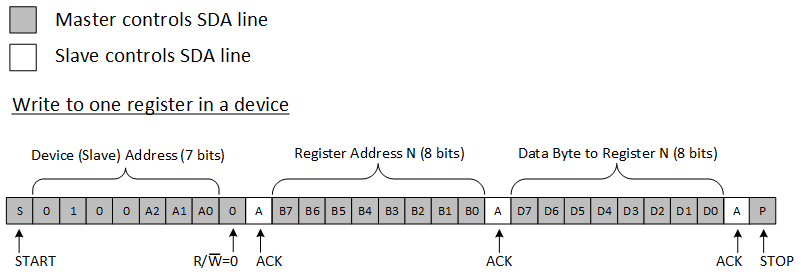
To write on the I2C bus, the master sends a START condition on the bus with the address of the slave, as well as the last bit (the R/W bit) set to 0, which signifies a write. After the slave sends the acknowledge bit, the master then sends the register address of the register to which it wishes to write. The slave acknowledges again, letting the master know it is ready. After this, the master starts sending the register data to the slave until the master has sent all the data necessary (which is sometimes only a single byte), and the master terminates the transmission with a STOP condition. Note that the command byte/register address does NOT automatically increment. Writing multiple bytes during a write results in the last byte sent being stored in the register.
See the Register Descriptions section to see list of the TCA9554's internal registers and a description of each one.
Figure 21 shows an example of writing a single byte to a slave register.
 Figure 21. Write to Register
Figure 22 shows an example of how to write to the polarity inversion register.
 Figure 22. Write to the Polarity Inversion Register
Figure 23 shows an example of how to write to output port register.
 Figure 23. Write to Output Port Register