ZHCSDP5E
December 2010 – February 2017
TCA9554A
PRODUCTION DATA.
1
特性
2
应用范围
3
说明
4
修订历史记录
5
Pin Configuration and Functions
6
Specifications
6.1
Absolute Maximum Ratings
6.2
ESD Ratings
6.3
Recommended Operating Conditions
6.4
Thermal Information
6.5
Electrical Characteristics
6.6
I2C Interface Timing Requirements
6.7
Switching Characteristics
6.8
Typical Characteristics
7
Parameter Measurement Information
8
Detailed Description
8.1
Overview
8.2
Functional Block Diagram
8.3
Feature Description
8.3.1
I/O Port
8.3.2
Interrupt Output (INT)
8.4
Device Functional Modes
8.4.1
Power-On Reset
8.5
Programming
8.5.1
I2C Interface
8.6
Register Maps
8.6.1
Device Address
8.6.2
Control Register and Command Byte
8.6.3
Register Descriptions
8.6.3.1
Bus Transactions
8.6.3.1.1
Writes
8.6.3.1.2
Reads
9
Application and Implementation
9.1
Application Information
9.2
Typical Application
9.2.1
Design Requirements
9.2.1.1
Calculating Junction Temperature and Power Dissipation
9.2.1.2
Minimizing ICC When I/Os Control LEDs
9.2.2
Detailed Design Procedure
9.2.3
Application Curves
10
Power Supply Recommendations
10.1
Power-On Reset Requirements
11
Layout
11.1
Layout Guidelines
11.2
Layout Example
12
器件和文档支持
12.1
文档支持
12.1.1
相关文档
12.2
接收文档更新通知
12.3
社区资源
12.4
商标
12.5
静电放电警告
12.6
Glossary
13
机械、封装和可订购信息
封装选项
机械数据 (封装 | 引脚)
DW|16
MSOI003I
PW|16
MPDS361A
DBQ|16
MSOI004H
DB|16
MPDS507A
散热焊盘机械数据 (封装 | 引脚)
DW|16
QFND313D
订购信息
zhcsdp5e_oa
zhcsdp5e_pm
7
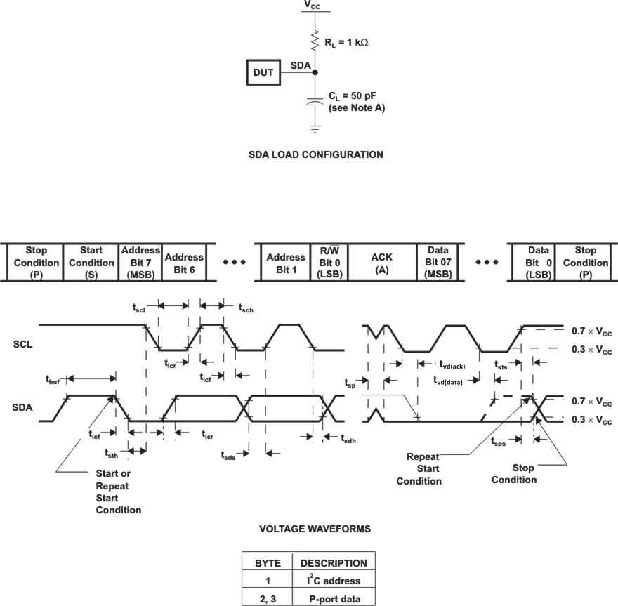
Parameter Measurement Information
A.
C
L
includes probe and jig capacitance.
B.
All inputs are supplied by generators having the following characteristics: PRR ≤ 10 MHz, Z
O
= 50 Ω, t
r
/t
f
≤ 30 ns.
C.
All parameters and waveforms are not applicable to all devices.
Figure 11.
I
2
C Interface Load Circuit and Voltage Waveforms
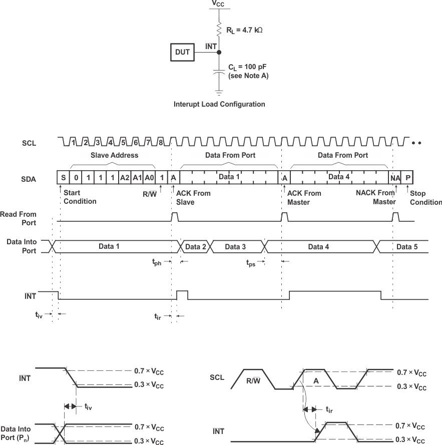
A.
C
L
includes probe and jig capacitance.
B.
All inputs are supplied by generators having the following characteristics: PRR ≤ 10 MHz, Z
O
= 50 Ω, t
r
/t
f
≤ 30 ns.
C.
All parameters and waveforms are not applicable to all devices.
Figure 12.
Interrupt Load Circuit and Voltage Waveforms
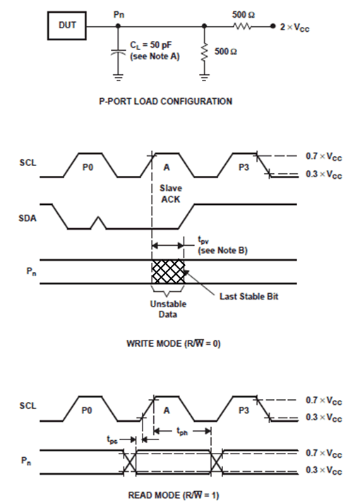
A.
C
L
includes probe and jig capacitance.
B.
t
pv
is measured from 0.7 × V
CC
on SCL to 50% I/O (Pn) output.
C.
All inputs are supplied by generators having the following characteristics: PRR ≤ 10 MHz, Z
O
= 50 Ω, t
r
/t
f
≤ 30 ns.
D.
The outputs are measured one at a time, with one transition per measurement.
E.
All parameters and waveforms are not applicable to all devices.
Figure 13.
P-Port Load Circuit and Voltage Waveforms
千亿体育app官网登录(中国)官方网站IOS/安卓通用版/手机APP
|
米乐app下载官网(中国)|ios|Android/通用版APP最新版
|
米乐|米乐·M6(中国大陆)官方网站
|
千亿体育登陆地址
|
华体会体育(中国)HTH·官方网站
|
千赢qy国际_全站最新版千赢qy国际V6.2.14安卓/IOS下载
|
18新利网v1.2.5|中国官方网站
|
bob电竞真人(中国官网)安卓/ios苹果/电脑版【1.97.95版下载】
|
千亿体育app官方下载(中国)官方网站IOS/安卓/手机APP下载安装
|