ZHCSG32B March 2017 – February 2020 TCA9800
PRODUCTION DATA.
- 1 特性
- 2 应用
- 3 说明
- 4 修订历史记录
- 5 Device Comparison Table
- 6 Pin Configuration and Functions
- 7 Specifications
- 8 Parameter Measurement Information
-
9 Detailed Description
- 9.1 Overview
- 9.2 Functional Block Diagram
- 9.3
Feature Description
- 9.3.1 Integrated Current Source
- 9.3.2 Ultra-Low Power Consumption
- 9.3.3 No Static-Voltage Offset
- 9.3.4 Active-High Repeater Enable Input
- 9.3.5 Powered Off High Impedance I2C Bus Pins on A-Side
- 9.3.6 Powered-Off Back-Power Protection for I2C Bus Pins
- 9.3.7 Clock Stretching and Multiple Master Arbitration Support
- 9.4 Device Functional Modes
- 10Application and Implementation
- 11Power Supply Recommendations
- 12Layout
- 13器件和文档支持
- 14机械、封装和可订购信息
7.8 Typical Characteristics
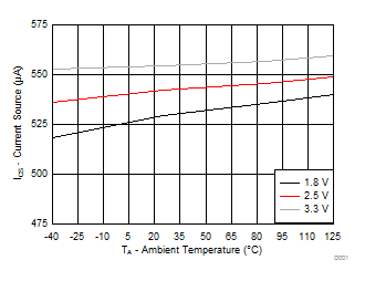
 Figure 1. Current Source vs Ambient Temperature for Different VCCB
  Figure 3. A-Side Output Low Voltage vs Low Level Current for Different TA (VCCB = 1.65 V)
  Figure 5. A-Side Output Low Voltage vs Low Level Current for Different TA (VCCB = 3.6 V)
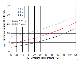
  Figure 7. Operating Current B-Side vs Ambient Temperature for Different VCCB (B-Side = VCCB)
  Figure 2. A-Side Output Low Voltage vs Ambient Temperature for Different VCCB (IOLA = 6 mA)
  Figure 4. A-Side Output Low Voltage vs Low Level Current for Different TA (VCCB = 2.5 V)
  Figure 6. Operating Current A-Side vs Ambient Temperature for Different VCCA (A-Side = VCCA & GND)
  Figure 8. Operating Current B-Side vs Ambient Temperature for Different VCCB (B-Side = GND)