ZHCSG41B March 2017 – February 2020 TCA9802
PRODUCTION DATA.
- 1 特性
- 2 应用
- 3 说明
- 4 修订历史记录
- 5 Device Comparison Table
- 6 Pin Configuration and Functions
- 7 Specifications
- 8 Parameter Measurement Information
-
9 Detailed Description
- 9.1 Overview
- 9.2 Functional Block Diagram
- 9.3
Feature Description
- 9.3.1 Integrated Current Source
- 9.3.2 Ultra-Low Power Consumption
- 9.3.3 No Static-Voltage Offset
- 9.3.4 Active-High Repeater Enable Input
- 9.3.5 Powered Off High Impedance I2C Bus Pins on A-Side
- 9.3.6 Powered-Off Back-Power Protection for I2C Bus Pins
- 9.3.7 Clock Stretching and Multiple Master Arbitration Support
- 9.4 Device Functional Modes
- 10Application and Implementation
- 11Power Supply Recommendations
- 12Layout
- 13器件和文档支持
- 14机械、封装和可订购信息
10.2.4.2 Detailed Design Procedure
Selecting the pull-up resistor required for the A-side (Bus A) is well documented already, see the I2C Bus Pullup Resistor Calculation application report. The rest of this section deals only with selection of a device based on the B-side design requirements.
Selection process of each device is identical to the procedure described in the Device Selection Guide section, except that it must be done for each individual TCA980x. This section jumps straight to the selection graphs to show the selection process. See the Detailed Design Procedure section for single device for detailed information.
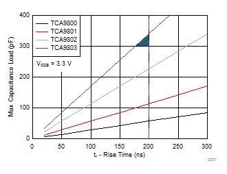
 Figure 35. Selection Guide Based On Example Design Requirements for Bus B
 Based on Figure 35, the TCA9803 is the only device which can satisfy the design requirements. Had the rise time requirement been ≤ 300 ns, then the TCA9802 also works, but the design requirement was 200 ns.
Based on Figure 36, all 4 variants of the TCA980x family meet the design requirements. The TCA9800 is the most optimized selection, but any of the variants can be used without issue.
As the system designer, the choice can be made to go for the most optimized part selections (TCA9803 for bus B and TCA9800 for bus C), but it is also ok to use the TCA9803 on both busses, because it can satisfy the design requirements of both busses.