ZHCSG42B March 2017 – February 2020 TCA9803
PRODUCTION DATA.
- 1 特性
- 2 应用
- 3 说明
- 4 修订历史记录
- 5 Device Comparison Table
- 6 Pin Configuration and Functions
- 7 Specifications
- 8 Parameter Measurement Information
-
9 Detailed Description
- 9.1 Overview
- 9.2 Functional Block Diagram
- 9.3
Feature Description
- 9.3.1 Integrated Current Source
- 9.3.2 Ultra-Low Power Consumption
- 9.3.3 No Static-Voltage Offset
- 9.3.4 Active-High Repeater Enable Input
- 9.3.5 Powered Off High Impedance I2C Bus Pins on A-Side
- 9.3.6 Powered-Off Back-Power Protection for I2C Bus Pins
- 9.3.7 Clock Stretching and Multiple Master Arbitration Support
- 9.4 Device Functional Modes
- 10Application and Implementation
- 11Power Supply Recommendations
- 12Layout
- 13器件和文档支持
- 14机械、封装和可订购信息
10.2.1 Single Device
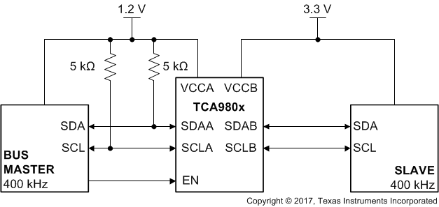
The typical application for the TCA980x family is to be used as a buffering translator, where the VCCA and VCCB are at different values in order to level-shift the I2C bus voltages.
It is critical to note that there are no external sources of current allowed on the B-side ports, since this can affect device operation as shown in the IEXT-I section.
 Figure 19. Typical Level-Shifting Application Example (Master on A-side)
 NOTE
Decoupling capacitors are not shown to keep the illustration simple. Decoupling capacitors (1 µF and 0.1 µF) must be placed close to each power supply pin.
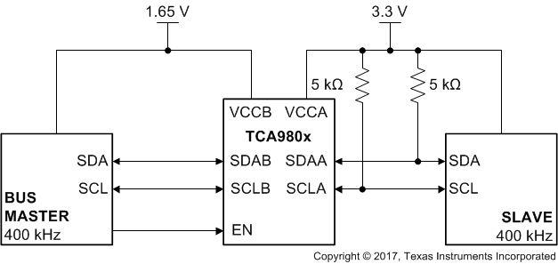
As shown in Figure 20, the I2C master can be on the B-side, and that it is ok to have VCCA > VCCB. The only requirements are that no external source of current (pull-up resistor or current source) be on the B-pins of the TCA980x, and that both VCCA/VCCB values are within the recommended range. As a note, since the EN pin is referenced to the VCCA supply voltage, when the master is on the A-side, the system designer must ensure that the enable pin voltage is pulled up to VCCA (either with an external or the internal pull-up resistor) to ensure that the device is enabled.
 Figure 20. Typical Level-Shifting Application Example (Master on B-side)
 NOTE
Decoupling capacitors are not shown to keep the illustration simple. Decoupling capacitors (1 µF and 0.1 µF) must be placed close to each power supply pin.