ZHCSG42B March   2017  – February 2020 TCA9803

PRODUCTION DATA.  

  1. 特性
  2. 应用
  3. 说明
    1.     Device Images
      1.      简化原理图
  4. 修订历史记录
  5. Device Comparison Table
  6. Pin Configuration and Functions
    1.     Pin Functions
  7. Specifications
    1. 7.1 Absolute Maximum Ratings
    2. 7.2 ESD Ratings
    3. 7.3 Recommended Operating Conditions
    4. 7.4 Thermal Information
    5. 7.5 Electrical Characteristics
    6. 7.6 Timing Requirements
    7. 7.7 Switching Characteristics
    8. 7.8 Typical Characteristics
  8. Parameter Measurement Information
  9. Detailed Description
    1. 9.1 Overview
    2. 9.2 Functional Block Diagram
    3. 9.3 Feature Description
      1. 9.3.1 Integrated Current Source
      2. 9.3.2 Ultra-Low Power Consumption
      3. 9.3.3 No Static-Voltage Offset
      4. 9.3.4 Active-High Repeater Enable Input
      5. 9.3.5 Powered Off High Impedance I2C Bus Pins on A-Side
      6. 9.3.6 Powered-Off Back-Power Protection for I2C Bus Pins
      7. 9.3.7 Clock Stretching and Multiple Master Arbitration Support
    4. 9.4 Device Functional Modes
      1. 9.4.1 Device Operation Considerations
        1. 9.4.1.1 B-Side Input Low (VIL/IILC/RILC)
          1. 9.4.1.1.1 VILC & IILC
          2. 9.4.1.1.2 RILC
        2. 9.4.1.2 Input and Output Leakage Current (IEXT-I/IEXT-O)
          1. 9.4.1.2.1 IEXT-I
          2. 9.4.1.2.2 IEXT-O
  10. 10Application and Implementation
    1. 10.1 Application Information
      1. 10.1.1 Device Selection Guide
      2. 10.1.2 Special Considerations for the B-side
        1. 10.1.2.1 FET or Pass-Gate Translators
        2. 10.1.2.2 Buffered Translators/Level-shifters
    2. 10.2 Typical Application
      1. 10.2.1 Single Device
        1. 10.2.1.1 Design Requirements
        2. 10.2.1.2 Detailed Design Procedure
        3. 10.2.1.3 Application Curves
      2. 10.2.2 Buffering Without Level-Shifting
        1. 10.2.2.1 Design Requirements
        2. 10.2.2.2 Detailed Design Procedure
        3. 10.2.2.3 Application Curve
      3. 10.2.3 Parallel Device Use Case
        1. 10.2.3.1 Design Requirements
        2. 10.2.3.2 Detailed Design Procedure
        3. 10.2.3.3 Application Curves
      4. 10.2.4 Series Device Use Case
        1. 10.2.4.1 Design Requirements
        2. 10.2.4.2 Detailed Design Procedure
        3. 10.2.4.3 Application Curve
  11. 11Power Supply Recommendations
  12. 12Layout
    1. 12.1 Layout Guidelines
    2. 12.2 Layout Example
  13. 13器件和文档支持
    1. 13.1 文档支持
    2. 13.2 接收文档更新通知
    3. 13.3 支持资源
    4. 13.4 商标
    5. 13.5 静电放电警告
    6. 13.6 Glossary
  14. 14机械、封装和可订购信息

封装选项

机械数据 (封装 | 引脚)
散热焊盘机械数据 (封装 | 引脚)
订购信息

Parallel Device Use Case

The TCA980x family supports multiple TCA980x used in parallel. The A-sides of the TCA980x are allowed to be connected together.

It is critical to note that there are no external sources of current allowed on the B-side ports, since this can affect device operation shown in the IEXT-I section.

NOTE: B-sides of TCA980x devices may never be connected to each other, because the IEXT-I specification limit is violated. See the IEXT-I section for more information.

NOTE: The B-side may not be connected to another translator if it uses a static-voltage offset. The RILC spec is violated since the static voltage offset adjusts the output resistance to ground to be outside of the RILC spec requirement, causing the TCA980x to be unable to recognize a low.
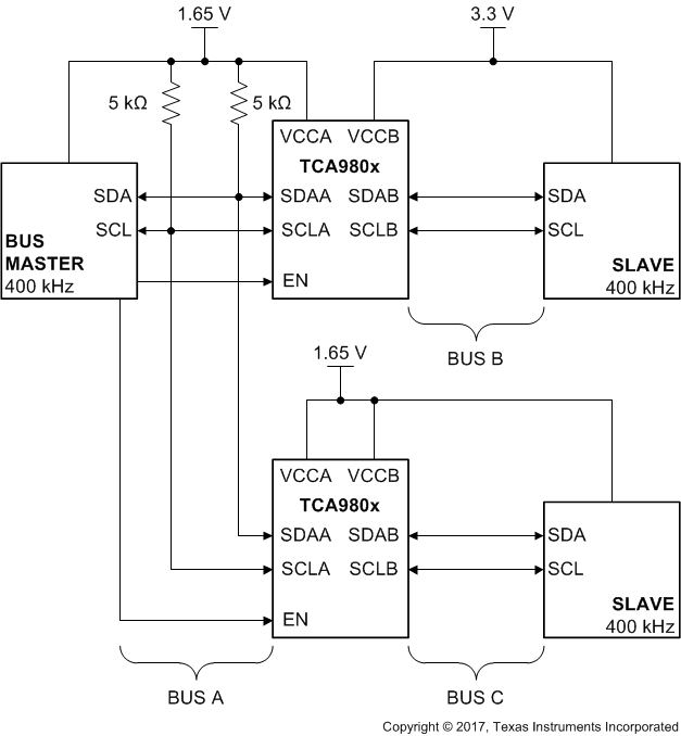
TCA9803 apps_parallel_trans.gifFigure 31. Parallel Use Case

NOTE

Decoupling capacitors are not shown to keep the illustration simple. Decoupling capacitors (1 µF and 0.1 µF) must be placed close to each power supply pin.