ZHCSP01 July   2022 TCAL9539

ADVANCE INFORMATION  

  1. 特性
  2. 应用
  3. 说明
  4. Revision History
  5. Pin Configuration and Functions
  6. Specifications
    1. 6.1 Absolute Maximum Ratings
    2. 6.2 ESD Ratings
    3. 6.3 Recommended Operating Conditions
    4. 6.4 Thermal Information
    5. 6.5 Electrical Characteristics
    6. 6.6 Timing Requirements
    7. 6.7 I2C Bus Timing Requirements
    8. 6.8 Switching Characteristics
  7. Parameter Measurement Information
  8. Detailed Description
    1. 8.1 Overview
    2. 8.2 Functional Block Diagrams
    3. 8.3 Feature Description
      1. 8.3.1 I/O Port
      2. 8.3.2 Adjustable Output Drive Strength
      3. 8.3.3 Interrupt Output (INT)
      4. 8.3.4 Reset Input (RESET)
      5. 8.3.5 Software Reset Call
    4. 8.4 Device Functional Modes
      1. 8.4.1 Power-On Reset
    5. 8.5 Programming
      1. 8.5.1 I2C Interface
    6. 8.6 Register Maps
      1. 8.6.1 Device Address
      2. 8.6.2 Control Register and Command Byte
      3. 8.6.3 Register Descriptions
      4. 8.6.4 Bus Transactions
        1. 8.6.4.1 Writes
        2. 8.6.4.2 Reads
  9. Application and Implementation
    1. 9.1 Application Information
    2. 9.2 Typical Application
      1. 9.2.1 Design Requirements
      2. 9.2.2 Detailed Design Procedure
        1. 9.2.2.1 Minimizing ICC When I/Os Control LEDs
      3. 9.2.3 Application Curves
    3. 9.3 Power Supply Recommendations
      1. 9.3.1 Power-On Reset Requirements
    4. 9.4 Layout
      1. 9.4.1 Layout Guidelines
      2. 9.4.2 Layout Example
  10. 10Device and Documentation Support
    1. 10.1 接收文档更新通知
    2. 10.2 支持资源
    3. 10.3 Trademarks
    4. 10.4 Electrostatic Discharge Caution
    5. 10.5 术语表
  11. 11Mechanical, Packaging, and Orderable Information
    1. 11.1 Tape and Reel Information
    2. 11.2 Mechanical Data

封装选项

机械数据 (封装 | 引脚)
散热焊盘机械数据 (封装 | 引脚)
订购信息

Reads

The bus controller first must send the TCAL9539 address with the LSB set to a logic 0 (see Figure 8-6 for device address). The command byte is sent after the address and determines which register is accessed.

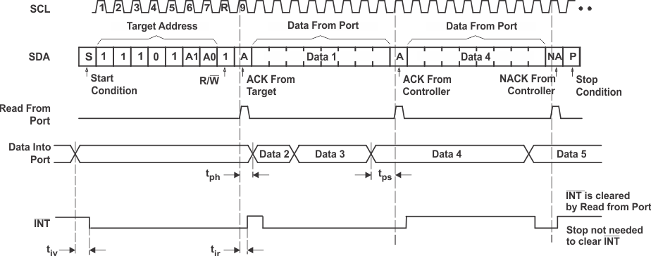
After a restart, the device address is sent again, but this time the least significant bit is set to a logic 1. Data from the register defined by the command byte is sent by the TCAL9539 (see Figure 8-10 and Figure 8-11). Data is clocked into the register on the rising edge of the ACK clock pulse. After the first byte is read, additional bytes may be read, but the data now reflects the information in the other register in the pair. For example, if Input Port 1 is read, the next byte read is Input Port 0.There is no limit on the number of data bytes received in one read transmission, but on the final byte received the bus master must not acknowledge the data. After a subsequent restart, the command byte contains the value of the next register to be read in the pair. For example, if Input Port 1 was read last before the restart, the register that is read after the restart is the Input Port 0.

GUID-20220128-SS0I-0FRW-SQF7-NMQTRDBFQXTW-low.gif Figure 8-10 Read From Register

GUID-20220128-SS0I-QCFN-BRMS-BHDWZTCPKBDD-low.gif
Transfer of data can be stopped at any time by a Stop condition. When this occurs, data present at the latest acknowledge phase is valid (output mode). It is assumed that the command byte previously has been set to 00 (read Input Port register).
This figure eliminates the command byte transfer, a restart, and responder address call between the initial responder address call and actual data transfer from P port (see Figure 8-10).
Figure 8-11 Read Input Port Register