ZHCSP01 July   2022 TCAL9539

ADVANCE INFORMATION  

  1. 特性
  2. 应用
  3. 说明
  4. Revision History
  5. Pin Configuration and Functions
  6. Specifications
    1. 6.1 Absolute Maximum Ratings
    2. 6.2 ESD Ratings
    3. 6.3 Recommended Operating Conditions
    4. 6.4 Thermal Information
    5. 6.5 Electrical Characteristics
    6. 6.6 Timing Requirements
    7. 6.7 I2C Bus Timing Requirements
    8. 6.8 Switching Characteristics
  7. Parameter Measurement Information
  8. Detailed Description
    1. 8.1 Overview
    2. 8.2 Functional Block Diagrams
    3. 8.3 Feature Description
      1. 8.3.1 I/O Port
      2. 8.3.2 Adjustable Output Drive Strength
      3. 8.3.3 Interrupt Output (INT)
      4. 8.3.4 Reset Input (RESET)
      5. 8.3.5 Software Reset Call
    4. 8.4 Device Functional Modes
      1. 8.4.1 Power-On Reset
    5. 8.5 Programming
      1. 8.5.1 I2C Interface
    6. 8.6 Register Maps
      1. 8.6.1 Device Address
      2. 8.6.2 Control Register and Command Byte
      3. 8.6.3 Register Descriptions
      4. 8.6.4 Bus Transactions
        1. 8.6.4.1 Writes
        2. 8.6.4.2 Reads
  9. Application and Implementation
    1. 9.1 Application Information
    2. 9.2 Typical Application
      1. 9.2.1 Design Requirements
      2. 9.2.2 Detailed Design Procedure
        1. 9.2.2.1 Minimizing ICC When I/Os Control LEDs
      3. 9.2.3 Application Curves
    3. 9.3 Power Supply Recommendations
      1. 9.3.1 Power-On Reset Requirements
    4. 9.4 Layout
      1. 9.4.1 Layout Guidelines
      2. 9.4.2 Layout Example
  10. 10Device and Documentation Support
    1. 10.1 接收文档更新通知
    2. 10.2 支持资源
    3. 10.3 Trademarks
    4. 10.4 Electrostatic Discharge Caution
    5. 10.5 术语表
  11. 11Mechanical, Packaging, and Orderable Information
    1. 11.1 Tape and Reel Information
    2. 11.2 Mechanical Data

封装选项

机械数据 (封装 | 引脚)
散热焊盘机械数据 (封装 | 引脚)
订购信息

Minimizing ICC When I/Os Control LEDs

When the I/Os are used to control LEDs, normally they are connected to V through a resistor as shown in Figure 9-2. For a P-port configured as an input, current consumption increases as VI becomes lower than V. The LED is a diode, with threshold voltage VT, and when a P-port is configured as an input the LED are off, but VI is a VT drop below VCC.

For battery-powered applications, it is essential that the voltage of P-ports controlling LEDs is greater than or equal to V when the P-ports are configured as input to minimize current consumption. Figure 9-2 shows a high-value resistor in parallel with the LED. Figure 9-3 shows V less than the LED supply voltage by at least VT. Both of these methods maintain the I/O VI at or above V and prevent additional supply current consumption when the P-port is configured as an input and the LED is off.
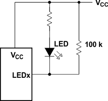
GUID-8A47F08E-69E9-4685-8A05-31DF3F4C429D-low.gif Figure 9-2 High-Value Resistor in Parallel with LED
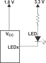
GUID-A512336E-7C8C-4BD4-9BF9-7C35B106F19C-low.gif Figure 9-3 Device Supplied by a Lower Voltage