ZHCSEK9D March 2016 – October 2021 TCAN1042H , TCAN1042HG , TCAN1042HGV , TCAN1042HV
PRODUCTION DATA
- 1 特性
- 2 应用
- 3 说明
- 4 Revision History
- 5 Device Comparison Table
- 6 Pin Configurations and Functions
- 7 Specifications
- 8 Parameter Measurement Information
-
9 Detailed Description
- 9.1 Overview
- 9.2 Functional Block Diagram
- 9.3 Feature Description
- 9.4 Device Functional Modes
- 10Application and Implementation
- 11Power Supply Recommendations
- 12Device and Documentation Support
- 13Mechanical, Packaging, and Orderable Information
6 Pin Configurations and Functions
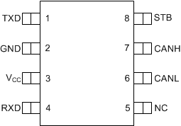
 Figure 6-1 D Package for Base, (H), (G) and (HG) Devices8 PIN (SOIC)Top View
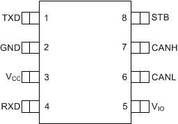
 Figure 6-3 D Package for (V), (HV), (GV), and (HGV) Devices8 PIN (SOIC)Top View
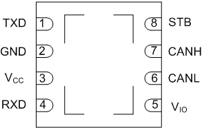
 Figure 6-2 DRB Package for Base, (H), (G) and (HG) Devices8 PIN (VSON)Top View
 Figure 6-4 DRB Package for (V), (HV), (GV), and (HGV) Devices8 PIN (VSON)Top View
Table 6-1 Pin Functions
| PINS | TYPE | DESCRIPTION | ||
|---|---|---|---|---|
| NAME | (H), (G), (HG) | (V), (GV), (HV), (HGV) | ||
| TXD | 1 | 1 | DIGITAL INPUT | CAN transmit data input (LOW for dominant and HIGH for recessive bus states) |
| GND(1) | 2 | 2 | GND | Ground connection |
| VCC | 3 | 3 | POWER | Transceiver 5-V supply voltage |
| RXD | 4 | 4 | DIGITAL OUTPUT | CAN receive data output (LOW for dominant and HIGH for recessive bus states) |
| NC | 5 | — | — | No Connect |
| VIO | — | 5 | POWER | Transceiver I/O level shifting supply voltage (Devices with "V" suffix only) |
| CANL | 6 | 6 | BUS I/O | Low level CAN bus input/output line |
| CANH | 7 | 7 | BUS I/O | High level CAN bus input/output line |
| STB | 8 | 8 | DIGITAL INPUT | Standby Mode control input (active high) |
(1) For DRB (VSON) package options, the thermal pad may be connected to GND in order to optimize the thermal characteristics of the package.